Semiconductor device and method of manufacturing semiconductor device

Active Publication Date: 2021-02-11
MITSUBISHI ELECTRIC CORP
View PDF0 Cites 0 Cited by
  • Summary
  • Abstract
  • Description
  • Claims
  • Application Information

AI Technical Summary

Benefits of technology

The patent describes a technique for improving heat dissipation in semiconductor devices by using a diamond substrate with a nitride semiconductor layer. The diamond substrate provides high heat conductivity, and the nitride semiconductor layer is formed on the upper surface of the diamond substrate. This helps to quickly transfer heat away from the semiconductor device, reducing its temperature and preventing malfunctions. The technique also includes a method of forming a groove in the semiconductor substrate to reduce stress and prevent cracks in the nitride semiconductor layer. Overall, the patent offers a simple and effective solution for improving the heat dissipation performance of semiconductor devices.

Problems solved by technology

However, temperature increase in the semiconductor device during high-output operation causes a problematic phenomenon of characteristic or reliability reduction of the device.

Method used


Image

  • Semiconductor device and method of manufacturing semiconductor device
  • Semiconductor device and method of manufacturing semiconductor device
  • Semiconductor device and method of manufacturing semiconductor device

Examples


first embodiment

[0046]A semiconductor device and a method of manufacturing the semiconductor device relating to the present embodiment will be described below.

[0047]

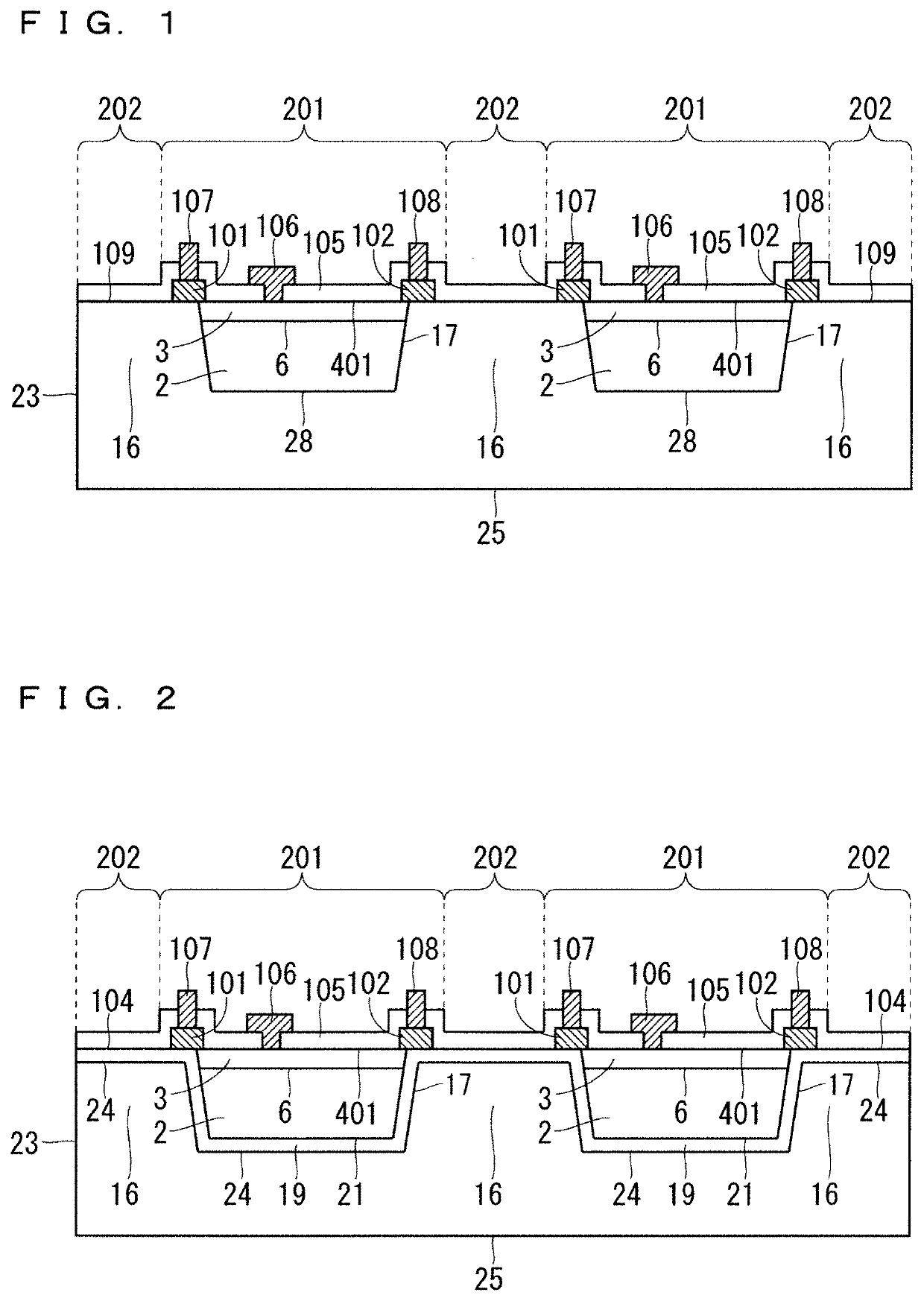
[0048]FIG. 1 is a cross-sectional view schematically showing an example of the configuration of the semiconductor device relating to the present embodiment. As shown in the example of FIG. 1, the semiconductor device includes: a diamond substrate 23 made of diamond; an epitaxial semiconductor layer 2 as a nitride semiconductor layer formed in a recess 17 of the diamond substrate 23; an epitaxial semiconductor layer 3 formed on the upper surface of the epitaxial semiconductor layer 2; a source or drain electrode metal 101 formed partially on an upper surface 401 of the epitaxial semiconductor layer 3; a drain or source electrode metal 102 formed partially on the upper surface 401 of the epitaxial semiconductor layer 3; a gate electrode metal 106 formed partially on the upper surface 401 of the epitaxial semiconductor layer 3; a surface p...

second embodiment

[0064]A semiconductor device and a method of manufacturing the semiconductor device relating to the present embodiment will be described below. In the description given below, a component similar to the component described in the foregoing embodiment will be given the same sign and illustrated with the same sign in the drawing. Detailed description of this component will be omitted, where appropriate.

[0065]

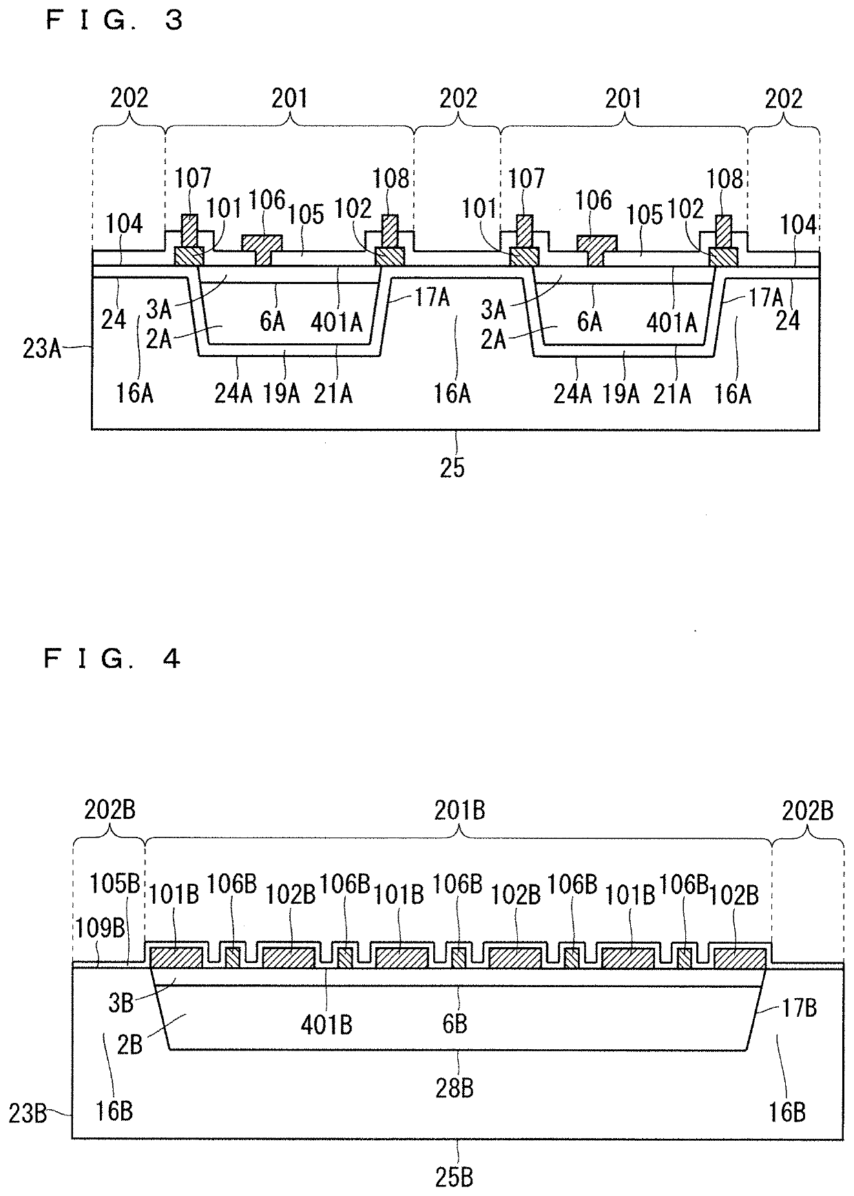
[0066]In FIG. 1, the epitaxial semiconductor layer 2 and the diamond substrate 23 directly contact each other. In a configuration described in the present embodiment, the epitaxial semiconductor layer 2 and the diamond substrate 23 do not directly contact each other.

[0067]FIG. 2 is a cross-sectional view schematically showing an example of the configuration of the semiconductor device relating to the present embodiment. As shown in the example of FIG. 2, the semiconductor device includes: the diamond substrate 23; an adhesion layer or a core forming layer 19 formed to cover the pr...

third embodiment

[0072]A semiconductor device and a method of manufacturing the semiconductor device relating to the present embodiment will be described below. In the description given below, a component similar to the component described in the foregoing embodiments will be given the same sign and illustrated with the same sign in the drawing. Detailed description of this component will be omitted, where appropriate.

[0073]

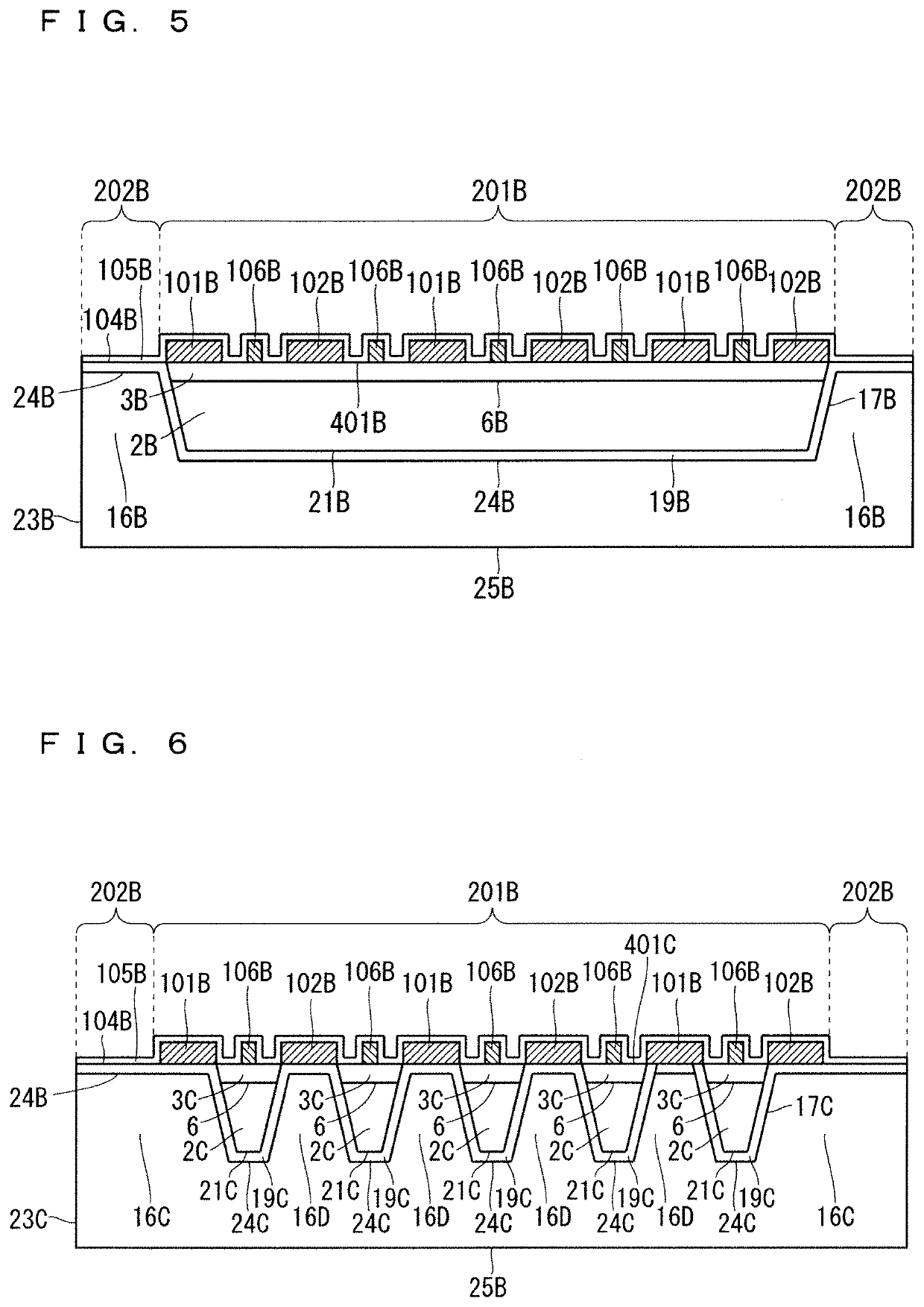
[0074]FIG. 3 is a cross-sectional view schematically showing another example of the configuration of the semiconductor device relating to the present embodiment. Unlike in the configurations shown in the examples of FIGS. 1 and 2, in the configuration show in the example of FIG. 3, the position of a projection 16A does not correspond to the element-to-element isolation region 202. Specifically, in the configuration shown in the example of FIG. 3, a recess 17A of a diamond substrate 23A has a narrow width, namely, the projection 16A of the diamond substrate 23A has a wide width. T...


PUM


Abstract

A technique disclosed in this description relates to a semiconductor device and a method of manufacturing the semiconductor device, and is intended to provide a semiconductor device having high heat dissipation performance. The semiconductor device relating to the technique disclosed in this description includes a diamond substrate and a nitride semiconductor layer. The diamond substrate is made of diamond. The nitride semiconductor layer is formed in a recess formed at an upper surface of the diamond substrate.

Description

TECHNICAL FIELD[0001]A technique disclosed in this description relates to a semiconductor device and a method of manufacturing the semiconductor device.BACKGROUND ART[0002]For example, a field-effect transistor made of a nitride-based semiconductor has conventionally been used as a high-output semiconductor device to operate in a high-frequency region. However, temperature increase in the semiconductor device during high-output operation causes a problematic phenomenon of characteristic or reliability reduction of the device.[0003]To suppress such temperature increase in the semiconductor device, it is important to provide a material of high heat dissipation performance or a structure of high heat dissipation performance near a part to generate heat. Diamond has the highest heat conductivity of those of solid substances and is used optimally as a material for heat dissipation.[0004]In a conventional semiconductor device using a diamond substrate, diamond is provided at least partial...

Claims


Application Information

Patent Timeline
IPC IPC(8): H01L23/373H01L29/20H01L29/778H01L29/66H01L21/02H01L21/48H01L21/78
CPCH01L23/3732H01L29/2003H01L29/7786H01L21/7806H01L21/02381H01L21/0254H01L21/4803H01L29/66462H01L29/778H01L29/0657H01L21/02002H01L29/812
Inventor YOSHITSUGU, KOJINAKAMURA, KEISUKEYAGYU, EIJI
Owner MITSUBISHI ELECTRIC CORP
Why Eureka
Try Eureka