Flexible display panel and flexible display device

Active Publication Date: 2021-03-18
WUHAN CHINA STAR OPTOELECTRONICS SEMICON DISPLAY TECH CO LTD
View PDF0 Cites 4 Cited by
  • Summary
  • Abstract
  • Description
  • Claims
  • Application Information

AI Technical Summary

Benefits of technology

[0016]In conclusion, in the embodiment of the present invention, the metal traces of the metal mesh do not surround each sub pixel in the organic light emitting diode layer for layout to reduce the arrangement density of the metal traces of the metal mesh, thus, the shielding of the light of the sub pixels by the metal traces of the metal mesh is reduced, so that the transmittance of the light emitted by the sub pixels is higher, thereby improving the overall display effect of the display area of the flexible display panel. In addition, a trace gap is arranged in at least one intersection of metal traces in each touch electrode. While the optical uniformity is maintained, the shiel

Problems solved by technology

However, indium tin oxide is used as a brittle semiconductor material and is not suitable for application for a flexible display screen.
However,

Method used


Image

  • Flexible display panel and flexible display device
  • Flexible display panel and flexible display device
  • Flexible display panel and flexible display device

Examples


first embodiment

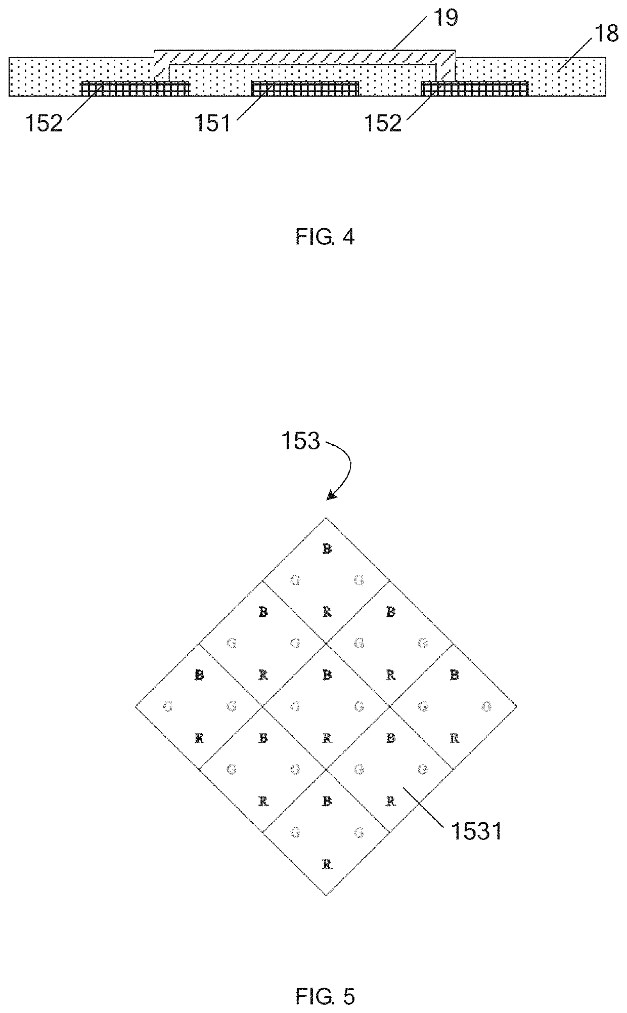
[0056]Please refer to FIG. 5. FIG. 5 is a structural diagram of a touch electrode according to the present invention. As an optional implementation, as shown in FIG. 5, at least one of the touch electrodes 153 comprises nine first touch areas 1531. Each of the first touch areas 1531 is correspondingly arranged with two green sub pixels G, one red sub pixel R and one blue sub pixel B. The two green sub pixels G, one red sub pixel R and one blue sub pixel B located in each of the first touch areas 1531 shown in FIG. 5 constitute one GRGB pixel unit. In other embodiments, the number and arrangement of the sub pixels corresponding to the first touch area 1531 are not limited thereto.

second embodiment

[0057]As another optional implementation, a number of sub pixels correspondingly arranged in a portion of the plurality of first touch areas 1531 is the same as shown in FIG. 6. Please refer to FIG. 6, FIG. 6 is a structural diagram of a touch electrode according to the present invention. As an optional implementation, as shown in FIG. 6, at least one of the touch electrodes 153 comprises six first touch areas 1531. The five first touch areas 1531 is correspondingly arranged with one GRGB pixel unit and one of the first touch areas 1531 is correspondingly arranged with four GRGB pixel units.

[0058]Please refer to FIG. 7 and FIG. 8. FIG. 7 is a structural diagram of a touch electrode according to the third embodiment of the present invention. FIG. 8 is a structural diagram of a touch electrode according to the fourth embodiment of the present invention. As an optional implementation, as shown in FIG. 7 or FIG. 8, at least one of the touch electrodes 153 comprises three first touch are...

fifth embodiment

[0061]Please refer to FIG. 9. FIG. 9 is a structural diagram of a touch electrode according to the present invention. As an optional implementation, as shown in FIG. 9, at least one of the touch electrodes 153 comprises six first touch areas 1531 and twelve second touch areas 1532. Each of the first touch areas 1531 is correspondingly arranged with one of the GRGB pixel units. It can be understood that the arrangements of the first touch areas 1531 and the second touch areas 1532 of the present invention are not limited to the arrangement shown in FIG. 9, and any other arrangements may be used. The repeated description is omitted here.

[0062]In one another specific embodiment, at least one of the touch electrodes 153 comprises only a plurality of the second touch areas 1532.


PUM


Abstract

Disclosed is a flexible display panel, comprising a flexible substrate; an organic light emitting diode layer, disposed on the flexible substrate, wherein the organic light emitting diode layer comprises a plurality of sub pixels arranged at intervals; a metal mesh, disposed on the organic light emitting diode layer, wherein metal traces of the metal mesh are correspondingly arranged in gaps among the plurality of sub pixels disposed at intervals, and the metal traces of the metal mesh surround to form a plurality of touch electrodes, and at least one of the touch electrodes comprises at least one first touch area, and the first touch area is correspondingly arranged with at least two of the sub pixels. The flexible display panel can improve the display effect of the flexible display panel by reducing the arrangement density of the metal traces of the metal mesh.

Description

CROSS-REFERENCE TO RELATED APPLICATION[0001]This application claims priority to Chinese Patent Application No. 201810134400.X entitled “Flexible display panel and flexible display device”, filed on Feb. 9, 2018, of which is hereby incorporated in its entirety by reference.FIELD OF THE INVENTION[0002]The present invention relates to a flexible display field, and more particularly to a flexible display panel and a flexible display device having the flexible display panel.BACKGROUND OF THE INVENTION[0003]Compared to the conventional display technologies such as liquid crystal display (LCD), the flexible displays possess many advantages, such as low power consumption, bendability, foldable property, thinness, portability and non-breakage. Particularly, a flexible active matrix organic light emitting diode (AMOLED) screen referred to as a next-generation display possesses advantages, such as wider viewing angle and thinner size and will be widely applied to smart phones, smart homes, wea...

Claims


Application Information

Patent Timeline
IPC IPC(8): G06F3/041H01L27/32G06F3/044H01L51/00
CPCG06F3/0412H01L27/323H01L27/3218G06F3/0446G06F2203/04111G06F2203/04102H01L2251/5338G06F2203/04112H01L51/0097G06F3/044H10K59/40G06F3/0443G06F2203/04103Y02E10/549H10K59/353H10K77/111H10K2102/311
Inventor YE, JIAN
Owner WUHAN CHINA STAR OPTOELECTRONICS SEMICON DISPLAY TECH CO LTD
Why Eureka
Try Eureka