Memory system and memory chip

a memory system and memory chip technology, applied in the field of memory system and memory chip, can solve the problems of less noise margin, faster data rate, and less noise margin of achieve the effect of improving the reading/writing window margin of the memory system

Pending Publication Date: 2021-04-08
ETRON TECH INC
View PDF3 Cites 3 Cited by
  • Summary
  • Abstract
  • Description
  • Claims
  • Application Information

AI Technical Summary

Benefits of technology

The present invention provides a memory system with two rows of pads for simultaneous data transmission and reception. The logic circuit uses the first aligned circuit, pads, and second aligned circuit to access data in parallel. This eliminates the need for additional circuits, reducing power and latency and improving reading and writing window margin.

Problems solved by technology

Due to stacked structures of the DRAM chips, scaling of the DRAM chips cannot follow scaling of the logic circuit.
However, the faster data rate has disadvantages (e.g. more expensive tester, less noise margin, and so on), and the wide data bus of the logic circuit and the wide data bus of the DRAM chips also have disadvantages (e.g. higher power, larger die area, and expensive Through-Silicon Via (“TSV”) process, and so on).
And no matter the aforesaid faster data rate of the DRAM or the wider data bus of the DRAM, all need serial-to-parallel circuit and parallel-to-serial circuit which increases clock latencies and power consumption.
Although the prior art can reduce the 4 clock latencies (e.g. 3.5 clock latencies) by optimizing the memory system 10, the above-mentioned serial-to-parallel converting process executed by the serial-to-parallel circuit 23 and the above-mentioned parallel-to-serial converting process executed by the parallel-to-serial circuit 314 would cost extra power, transmission latencies, and die areas, result in low efficiencies of the memory system 10.
Therefore, how to reduce cost of the power, transmission latencies, and die areas becomes an important issue for a designer of the memory system.

Method used


Image

  • Memory system and memory chip
  • Memory system and memory chip
  • Memory system and memory chip

Examples


Embodiment Construction

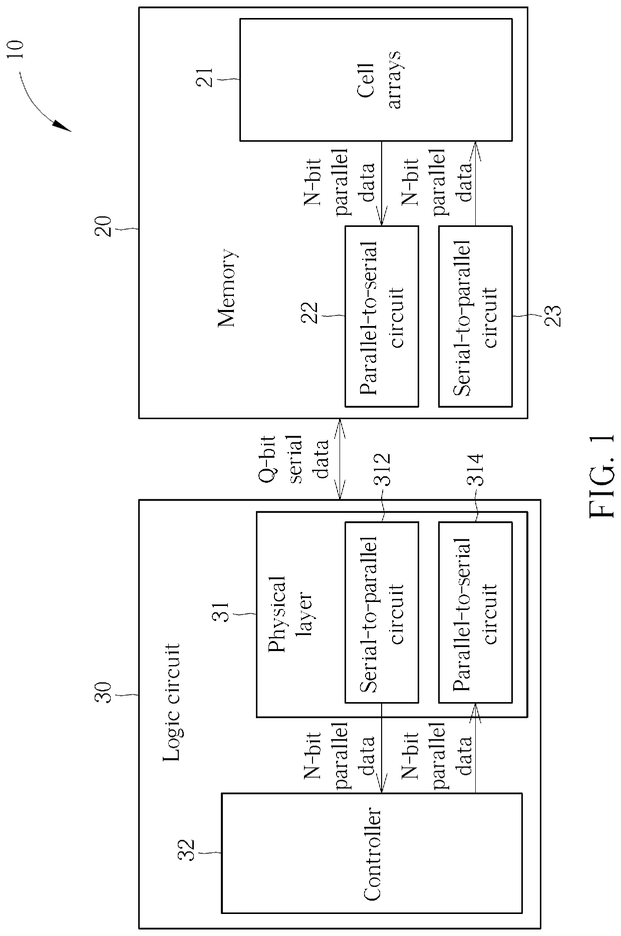
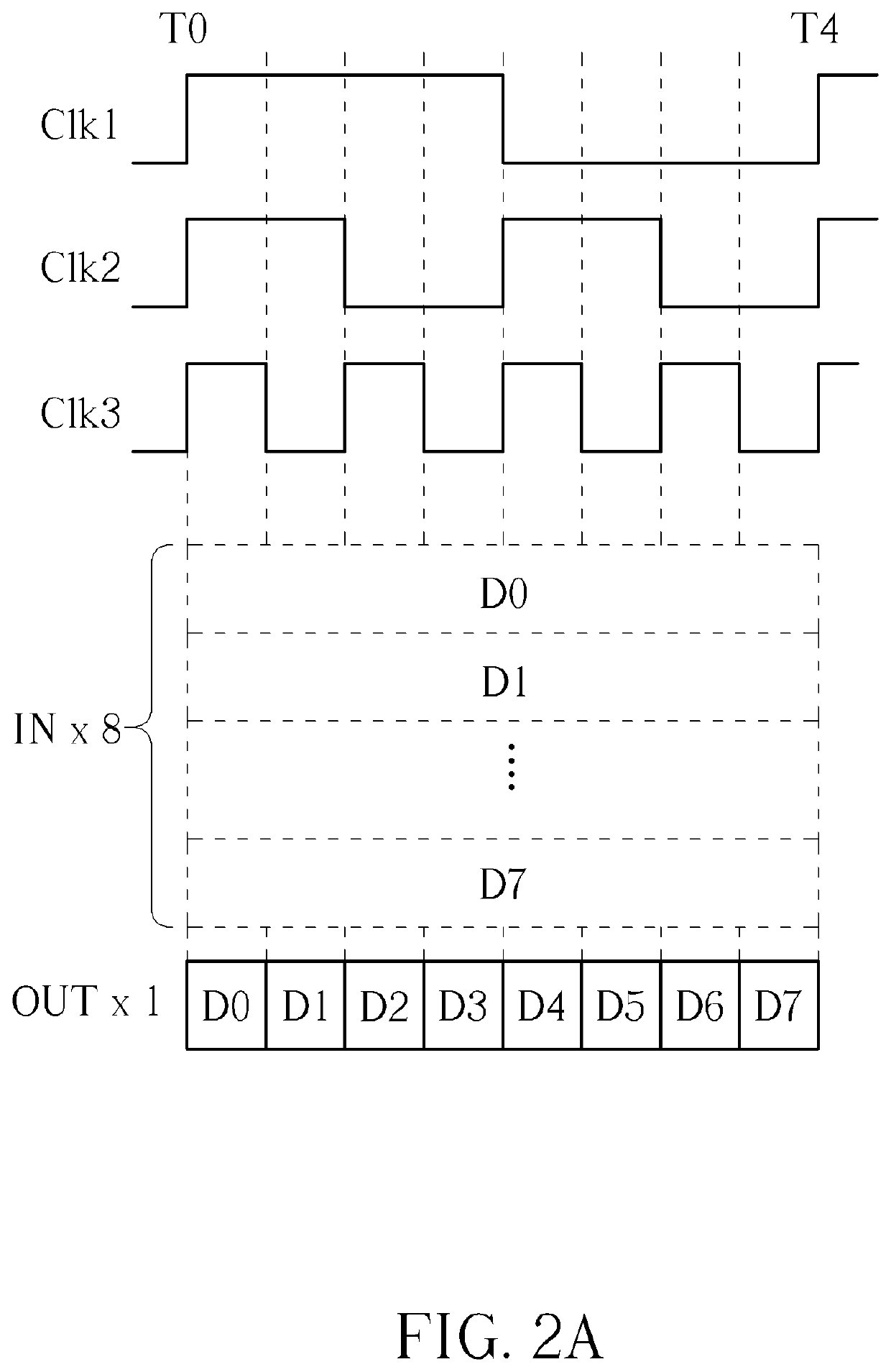
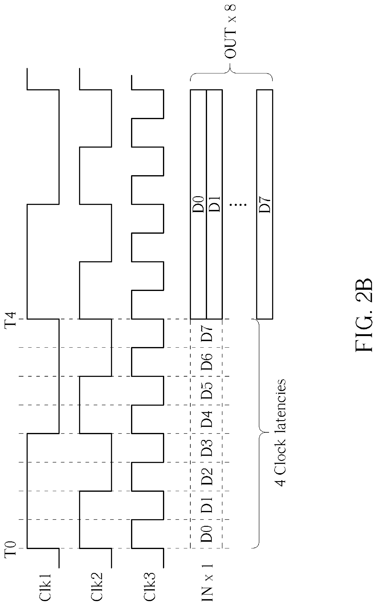
[0043]Please refer to FIG. 3. FIG. 3 is a diagram illustrating a memory system 100 according to a first embodiment of the present invention. As shown in FIG. 3, the memory system 100 includes a memory 101 and a logic circuit 102, wherein the memory 101 can be a dynamic random access memory (DRAM), a static random access memory (SRAM), a flash memory or other kinds of memories, and the logic circuit 102 can be an artificial intelligence (AI) chip or a system on chip (SOC). In addition, in one embodiment of the present invention, the memory 101 can include a base DRAM chip and a plurality of DRAM chips stacked above the base DRAM chip. In addition, the logic circuit 102 is coupled to other devices or processors through an AXI (Advanced extensible Interface) bus, wherein the AXI bus is a bus protocol, the protocol is part of the AMBA (Advanced Microcontroller Bus Architecture) 3.0 protocol. The AXI bus includes a writing data bus and a reading data bus. In addition, an operation method...


PUM


Abstract

A memory chip includes a memory bank, an I / O data bus, and a first plurality of sensing amplifiers. The first plurality of sensing amplifiers is configured to parallelly output a first plurality of data. A width of the I / O data bus is equal to a width of the first plurality of data parallelly outputted by the first plurality of sensing amplifiers.

Description

CROSS REFERENCE TO RELATED APPLICATIONS[0001]This application claims the benefit of U.S. Provisional Application No. 62 / 910,468, filed on Oct. 4, 2019 and entitled “Novel DRAM System”, and the benefit of U.S. Provisional Application No. 63 / 007,960, filed on Apr. 10, 2020 and entitled “Better dram system,” the contents of which are incorporated herein by reference.BACKGROUND OF THE INVENTION1. Field of the Invention[0002]The present invention relates to a memory system and a memory chip, and particularly to a memory system and a memory chip that can let data be transmitted between a logic circuit and the memory chip in parallel.2. Description of the Prior Art[0003]Nowadays, a memory system for high performance computing or artificial intelligence (AI) system usually includes dynamic random access memory (DRAM) chips and a logic circuit. Due to stacked structures of the DRAM chips, scaling of the DRAM chips cannot follow scaling of the logic circuit. Therefore, a memory-wall effect oc...

Claims


Application Information

Patent Timeline
Patent Type & Authority Applications(United States)
IPC IPC(8): G06F13/16G11C11/4091G11C11/4093
CPCG06F13/1678G11C11/4093G11C11/4091G11C7/06G11C7/1051G11C7/1078H03M9/00G11C2207/107G11C2207/108G11C11/4096G11C7/1012G11C7/106G11C7/1066G11C7/1087G11C7/1093
Inventor SHIAH, CHUN
Owner ETRON TECH INC
Why Eureka
Try Eureka