
Organic light emitting diode and organic light emitting device including the same

a light-emitting diode and organic technology, applied in the direction of luminescent compositions, semiconductor devices, luminescent compositions, etc., can solve the problems of low luminous efficiency of conventional fluorescent materials, too short luminous lifetime of metal complexes as representative phosphorescent materials to be applicable into commercial devices, etc., to enhance luminous efficiency and lifetime, and reduce the driving voltage

Pending Publication Date: 2021-04-22
LG DISPLAY CO LTD
View PDF4 Cites 0 Cited by
  • Summary
  • Abstract
  • Description
  • Claims
  • Application Information

AI Technical Summary

Benefits of technology

The patent aims to provide an OLED that can reduce the voltage needed to operate it, while also making it brighter and longer-lasting. The invention is a type of organic light emitting diode.

Problems solved by technology

Conventional fluorescent materials have shown low luminous efficiency because only the singlet excitons are involved in the luminescence process thereof.
However, the metal complex as the representative phosphorescent material has too short luminous lifetime to be applicable into commercial devices.

Method used


Image

  • Organic light emitting diode and organic light emitting device including the same
  • Organic light emitting diode and organic light emitting device including the same
  • Organic light emitting diode and organic light emitting device including the same

Examples


example 1 (

Ex. 1): Fabrication of OLED

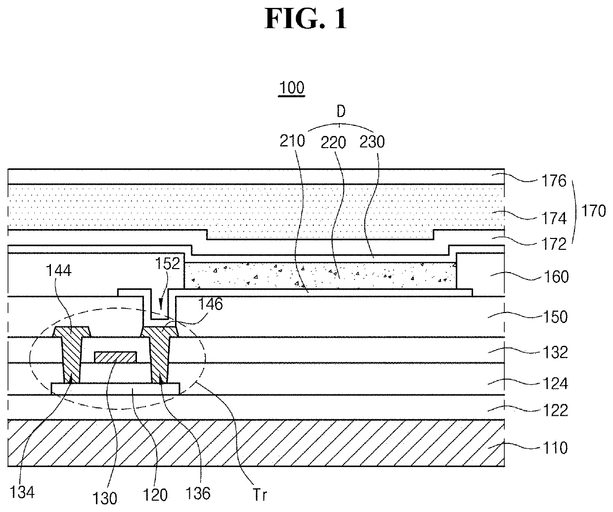
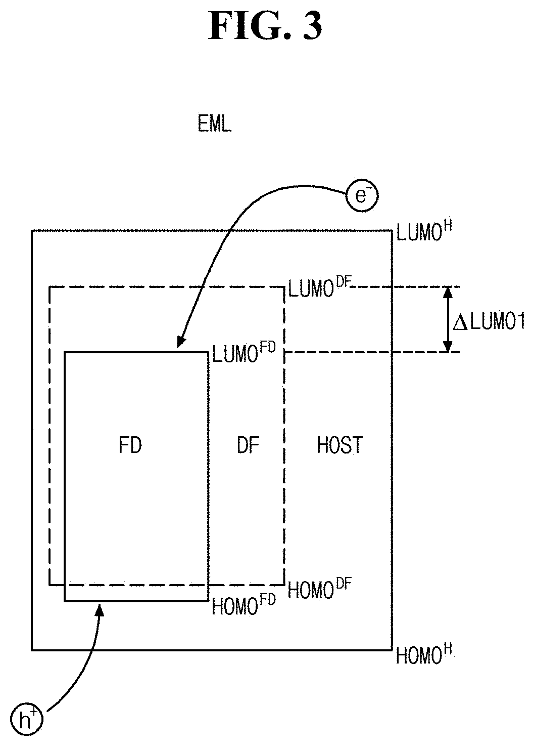
[0217]An OLED comprising an EML into which mCBP (LUMO −2.5 eV; HOMO −6.0 eV) as a host, compound 1-1 (LUMO −3.0 eV; HOMO −5.7 eV) in Chemical Formula 2 as delayed fluorescent material (DF) and compound 2-1 (LUMO −3.6 eV; HOMO −5.8 eV) in Chemical Formula 4 as fluorescent material (FD) was introduced was fabricated. ITO substrate was washed by UV-Ozone treatment before using, and was transferred to a vacuum chamber for depositing emission layer. Subsequently, an anode, an emission layer and a cathode were deposited by evaporation from a heating boat under 104 torr vacuum condition with setting deposition rate of 1 Å / s in the following order:

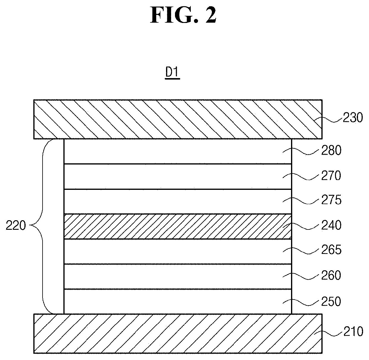
[0218]An anode (ITO, 50 nm); a HIL (HAT-CN, 7 nm); a HTL (NPB, 78 nm); an EBL (TAPC, 15 nm), an EML (mCBP:Compound 1-1:Compound 2-1=64:35:1 by weight ratio, 35 nm); a HBL (B3PYMPM, 10 nm); an ETL (TPBi, 25 nm), an EIL (LiF); and a cathode (Al).

[0219]And then, cappling layer (CPL) was deposited over the cathode and the de...

example 2 (

Ex. 2): Fabrication of OLED

[0220]An OLED was fabricated using the same materials as Example 1, except that compound 1-2 (LUMO −3.1 eV; HOMO −5.7 eV) in Chemical Formula 2 was used as delayed fluorescent material in the EML instead of compound 1-1. LUMOFD−LUMODF=−0.5 eV; HOMOFD−HOMODF=−0.1 eV.

example 3 (

Ex. 3): Fabrication of OLED

[0221]An OLED was fabricated using the same materials as Example 1, except that compound 1-17 (LUMO −3.1 eV; HOMO −5.9 eV) in Chemical Formula 2 was used as delayed fluorescent material in the EML instead of compound 1-1. LUMOFD−LUMODF=−0.5 eV; HOMOFD−HOMODF=0.1 eV.


PUM

PropertyMeasurementUnit
voltageaaaaaaaaaa
energy level bandgap ΔESTDFaaaaaaaaaa

Abstract

An organic light emitting diode (OLED) including at least one emitting material layer (EML) disposed two electrodes and comprising triazine-based delayed fluorescent material and boron-dipyrromethene-based fluorescent material and an organic light emitting device including the OLED is disclosed. The triazine-based delayed fluorescent material and the boron-dipyrromethene-based fluorescent material may be included in an identical EML or in adjacently disposed EMLs. The OLED can lower its driving voltage and improve its luminous efficiency by adjusting energy levels of the delayed fluorescent material and the fluorescent material.

Description

CROSS-REFERENCE TO RELATED APPLICATIONS[0001]This application claims the benefit under 35 U.S.C. § 119(a) to Korean Patent Application No. 10-2019-0129775, filed in the Republic of Korea on Oct. 18, 2019 and No. 10-2020-0113952, filed in the Republic of Korea on Sep. 7, 2020, the entire contents of which are incorporated herein by reference into the present application.BACKGROUNDTechnical Field[0002]The present disclosure relates to an organic light emitting diode, and more specifically, to an organic light emitting diode having excellent luminous properties and an organic light emitting device having the diode.Discussion of the Related Art[0003]As display devices have become larger, there exists a need for a flat display device with lower spacing occupation. Among the flat display devices, a display device using an organic light emitting diode (OLED) has come into the spotlight.[0004]In the OLED, when electrical charges are injected into an emitting material layer between an electr...

Claims


Application Information

Patent Timeline
Patent Type & Authority Applications(United States)
IPC IPC(8): H01L51/00
CPCH01L51/0067H01L51/5004H01L51/008H10K59/12H10K85/322H10K85/654H10K85/657H10K50/131H10K85/6572H10K50/11C09K11/06C09K2211/107C09K2211/1055
Inventor LEE, JI-AEKIM, JUN-YUNHONG, TAE-RYANGBAEK, JEONG-EUN
Owner LG DISPLAY CO LTD
Learn More