Ferroelectric semiconductor device and method for producing a memory cell

Active Publication Date: 2021-05-20
FRAUNHOFER GESELLSCHAFT ZUR FOERDERUNG DER ANGEWANDTEN FORSCHUNG EV +1
View PDF26 Cites 5 Cited by
  • Summary
  • Abstract
  • Description
  • Claims
  • Application Information

AI Technical Summary

Benefits of technology

This patent is about a type of semiconductor device that uses a special mixed crystal to store information. This mixed crystal has good stability and can be used to store data that can be recalled even at high temperatures. This type of device also has good scalability, meaning it can store more data in a smaller space. The patent also mentions an integrated circuit that includes this type of semiconductor device, which ensures reliable and long-term storage of data.

Problems solved by technology

However, an obvious disadvantage is that information is not stored permanently and is thus not available, e.g., after a restart of a device.
However, conventional non-volatile media, which do not have this problem, have significantly slower switching times (time that is needed to write an information unit).
Significant obstacles, which have up to now prevented commercially successful components, are an unsatisfactory long-term stability as well as lack of compatibility with standard CMOS processes (CMOS=complementary metal-oxide-semiconductor).
Many of the more significant ferroelectrics are perovskite oxides having typical disadvantages such as low paraelectric transition temperatures, non-linear shifts or compatibility problems with the complementary metal-oxide semiconductor (CMOS) technology [2, 4].

Method used


Image

  • Ferroelectric semiconductor device and method for producing a memory cell
  • Ferroelectric semiconductor device and method for producing a memory cell
  • Ferroelectric semiconductor device and method for producing a memory cell

Examples


Embodiment Construction

[0050]Before embodiments of the present invention will be discussed below in detail based on the drawings, it should be noted that identical, functionally equal or equal elements, objects and / or structures are provided with the same or similar reference numbers in the different figures, such that the description of these elements illustrated in the different embodiments is inter-exchangeable or inter-applicable.

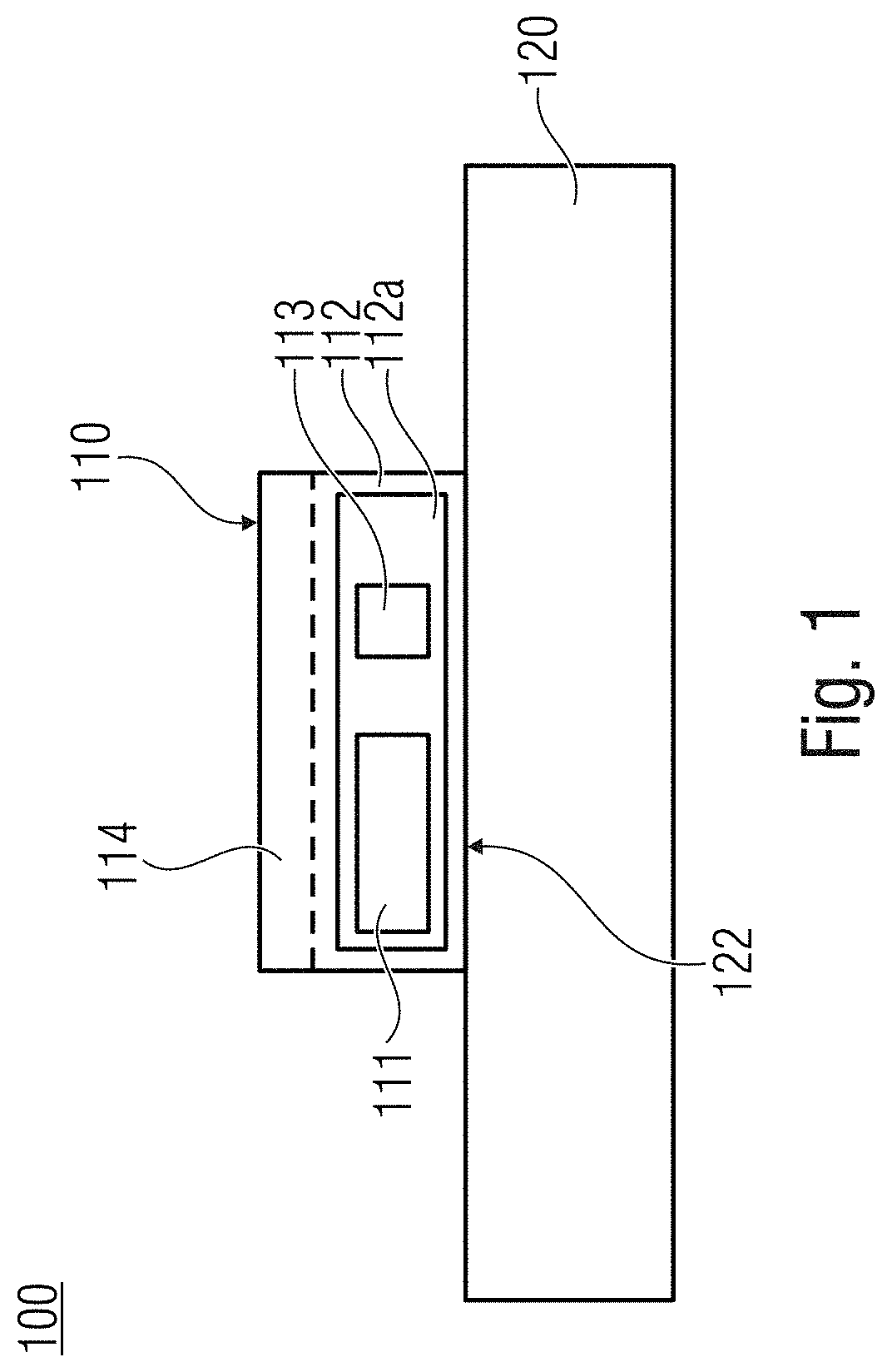
[0051]FIG. 1 shows a schematic illustration of ferroelectric semiconductor device 100 with a memory cell 110 and a semiconductor device 120 connected to the memory cell 110. The memory cell 110 can comprise a ferroelectric memory layer 112 and a first conductive layer 114 disposed on the ferroelectric memory layer 112. The ferroelectric memory layer 112 of the memory cell 110 can comprise a mixed crystal 112a with a group III nitride 111 and a non-group III element 113. Thus, the ferroelectric semiconductor device 100 can comprise a first group III nitride-based ferroelectric...


PUM


Abstract

Ferroelectric semiconductor device with a memory cell, with a ferroelectric memory layer and a first conductive layer disposed on the ferroelectric memory layer; and a semiconductor device connected to the memory cell. The ferroelectric memory layer of the memory cell can include a mixed crystal with a group III nitride and a non-group III element.

Description

CROSS-REFERENCE TO RELATED APPLICATIONS[0001]This application is a continuation of copending International Application No. PCT / EP2019 / 069963, filed Jul. 24, 2019, which is incorporated herein by reference in its entirety, and additionally claims priority from German Application No. 10 2018 212 736.0, filed Jul. 31, 2018, which is also incorporated herein by reference in its entirety.[0002]Embodiments according to the invention relate to a ferroelectric semiconductor device and a method for producing a memory cell.BACKGROUND OF THE INVENTION[0003]Memory cells used in integrated circuits can be divided in volatile and non-volatile principles. As volatile elements, dynamic random access memories (DRAM) are to be mentioned. The same have a fast switching behavior and can be produced with very large density. However, an obvious disadvantage is that information is not stored permanently and is thus not available, e.g., after a restart of a device. However, conventional non-volatile media,...

Claims


Application Information

Patent Timeline
IPC IPC(8): H01L27/1159H01L29/51H01L29/78H01L21/28H01L29/66
CPCH01L27/1159H01L29/516H01L29/6684H01L29/40111H01L29/78391G11C11/223H01L29/2003H10B51/30
Inventor WAGNER, BERNHARDFICHTNER, SIMONLOFINK, FABIAN
Owner FRAUNHOFER GESELLSCHAFT ZUR FOERDERUNG DER ANGEWANDTEN FORSCHUNG EV
Why Eureka
Try Eureka