Method for forming an electronic product comprising two capacitors having different dielectric thicknesses, and corresponding electronic product

a technology of dielectric thickness and capacitor, which is applied in the field of integration, can solve the problems of reducing the capacitance per unit of surface of the device, consuming a significant area of silicon, and high value capacitance, and achieves the effects of low deposition rate, high deposition rate and high deposition ra

Pending Publication Date: 2021-07-01
MURATA MFG CO LTD
View PDF0 Cites 0 Cited by
  • Summary
  • Abstract
  • Description
  • Claims
  • Application Information

AI Technical Summary

Benefits of technology

[0028]It has been observed by the inventors that depositing a protective layer using, for example, PECVD, allows depositing a layer in a possibly non conformal manner which obstructs any blind hole or trench between pillars. A quick deposition of material may then prevent the deposition of dielectric in the areas covered by the protective layer.
[0029]It should be noted that PECVD is a technique that enables the deposition of thick films (1 μm range) with a high deposition rate at low temperature (&

Problems solved by technology

However planar capacitors provide low capacitance density, this implies that a high value capacitance will consume a significant area of silicon.
This may reduce the

Method used


Image

  • Method for forming an electronic product comprising two capacitors having different dielectric thicknesses, and corresponding electronic product
  • Method for forming an electronic product comprising two capacitors having different dielectric thicknesses, and corresponding electronic product
  • Method for forming an electronic product comprising two capacitors having different dielectric thicknesses, and corresponding electronic product

Examples


Embodiment Construction

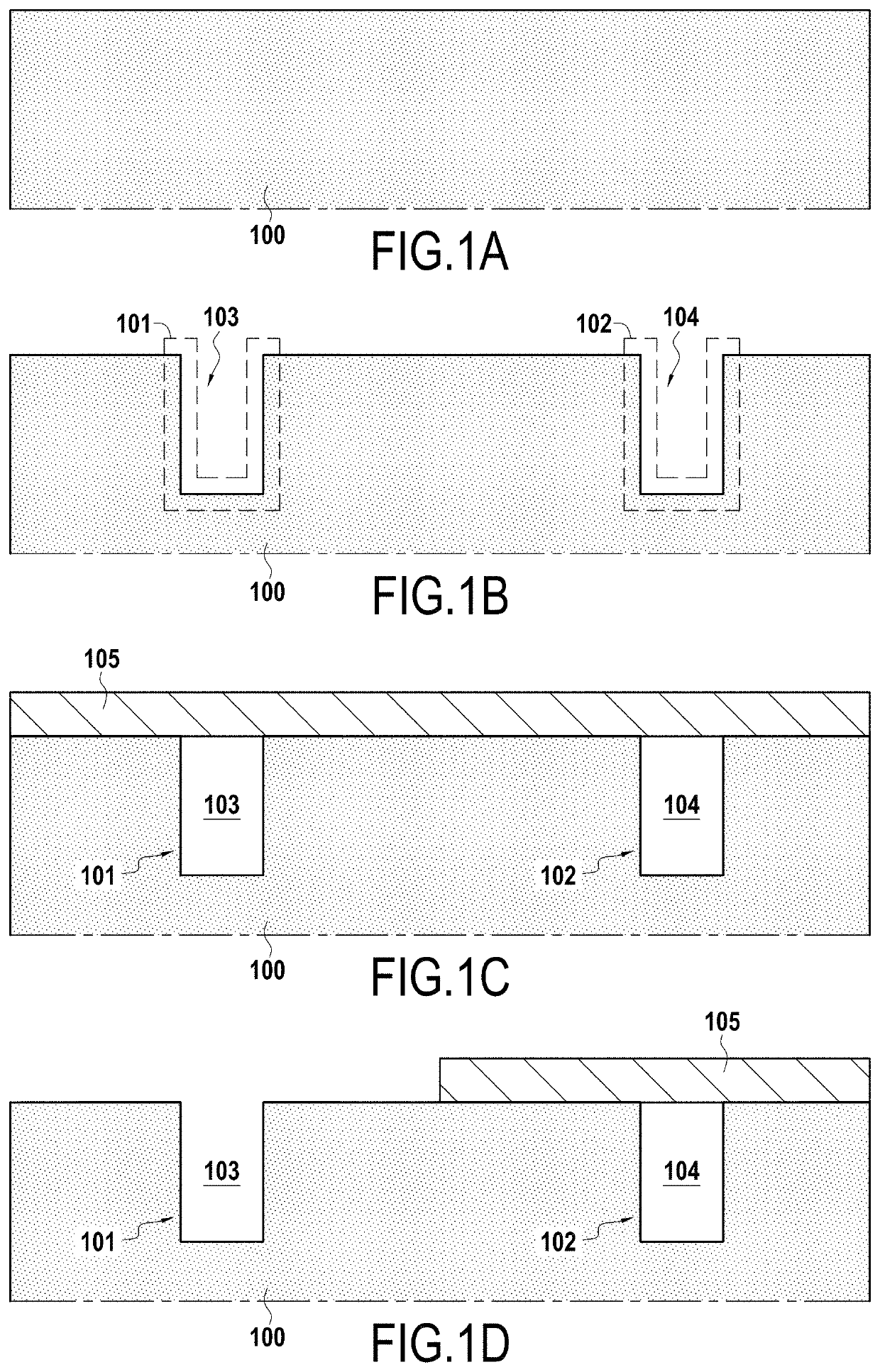
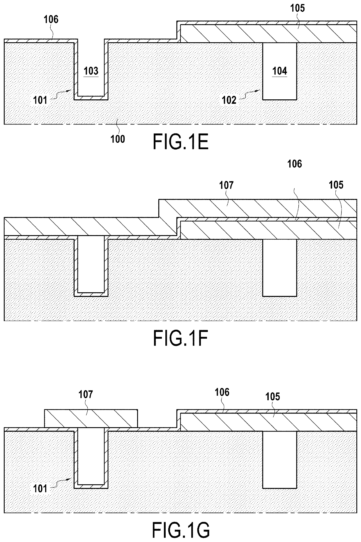
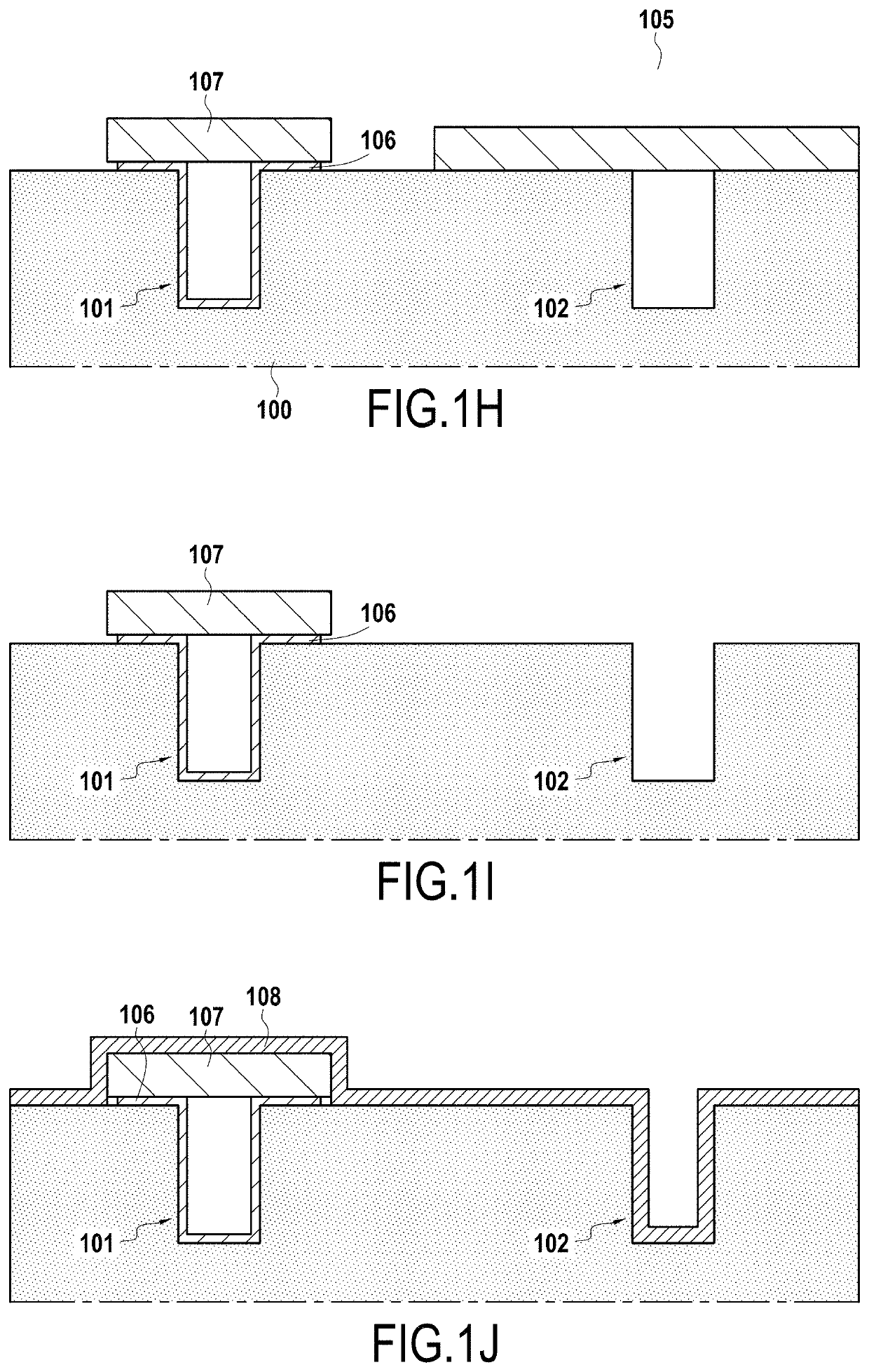
lass="d_n">[0049]The steps for fabricating this electronic product comprising two capacitors having different dielectric thicknesses according to an embodiment will be described hereinafter.

[0050]FIG. 1A is a side view of a semi-conductor substrate 100, and in this example the substrate is a silicon substrate. This substrate typically has a thickness of the order of several hundreds of micrometers.

[0051]In order to form a capacitor, bottom electrodes are formed in the silicon substrate from the top surface (on the figure) of the substrate, as shown on FIG. 1B. On this figure a first bottom electrode 101 and a second bottom electrode 102. The manufacture of these electrodes comprises carrying out a DRIE step on the top of the surface of the substrate 100. This DRIE step forms, in this example, two holes 103 and 104 respectively associated with the first bottom electrode 101 and the second bottom electrode 103.

[0052]It should be noted that the invention is not limited to electrodes co...


PUM


Abstract

An electronic product having a first capacitor and a second capacitor, where the electronic product includes a semi-conductor substrate having a bottom electrode region of the first capacitor and a bottom electrode region of the second capacitor; a first dielectric layer having a first thickness arranged above the bottom electrode region of the first capacitor; a second dielectric layer having a second thickness arranged above the bottom electrode region of the second capacitor, the first thickness and the second thickness being different; a top electrode region of the first capacitor arranged above the bottom electrode of the first capacitor and above the first dielectric layer; and a top electrode region of the second capacitor arranged above the bottom electrode of the second capacitor and above the second dielectric layer.

Description

CROSS REFERENCE TO RELATED APPLICATIONS[0001]The present application is a continuation of International application No. PCT / IB2019 / 057139, filed Aug. 26, 2019, which claims priority to European Patent Application No. 18 306 164.7, filed Sep. 4, 2018, the entire contents of each of which are incorporated herein by referenceFIELD OF THE INVENTION[0002]The present invention relates to the field of integration and, more particularly, to electronic products, related semiconductor products, and their methods of manufacture.[0003]The present invention more precisely relates to electronic components comprising capacitors.TECHNICAL BACKGROUND[0004]Electronic components such as capacitors may be integrated into semiconductor products in a variety of forms. For example, planar capacitors may be formed above semiconductor substrates by forming two planar electrodes separated by a dielectric layer. However planar capacitors provide low capacitance density, this implies that a high value capacita...

Claims


Application Information

Patent Timeline
IPC IPC(8): H01L49/02H01L21/3065H01L21/311
CPCH01L28/91H01L21/31111H01L21/3065H01L27/0805H01L29/66181H01L29/945
Inventor LALLEMAND, FLORENTBOUVIER, STÉPHANE
Owner MURATA MFG CO LTD
Why Eureka
Try Eureka