Process and apparatus for preparing amorphous hydrosilicon film

A silicon thin film and amorphous technology is applied in the field of preparing amorphous hydrogen silicon thin films and devices, and can solve the problems of performance damage of semiconductor devices, low deposition rate of a-Si:H thin films, restriction of gas flow rate of reaction precursors, etc.

Inactive Publication Date: 2007-11-07
ZHEJIANG UNIV
View PDF2 Cites 15 Cited by
  • Summary
  • Abstract
  • Description
  • Claims
  • Application Information

AI Technical Summary

Problems solved by technology

However, the working pressure required by this radio frequency discharge mode is low (about 100Pa), which limits the gas flow rate of the reaction precursor, and the deposition rate of a-Si:H film is low (about 5-10nm / min).
In addition, the average energy of electrons provided by radio frequency discharge is low (<1eV), so that the substrate temperature when depositing a-Si:H film needs to be at least 200 ° C, which limits the selection of a variety of low melting point substrate materials. On the one hand, impurities such as carbon and heavy metals on the substrate may diffuse into the formed film during the heating process, causing damage to the performance of semiconductor devices

Method used


Image

  • Process and apparatus for preparing amorphous hydrosilicon film

Examples


Embodiment 1

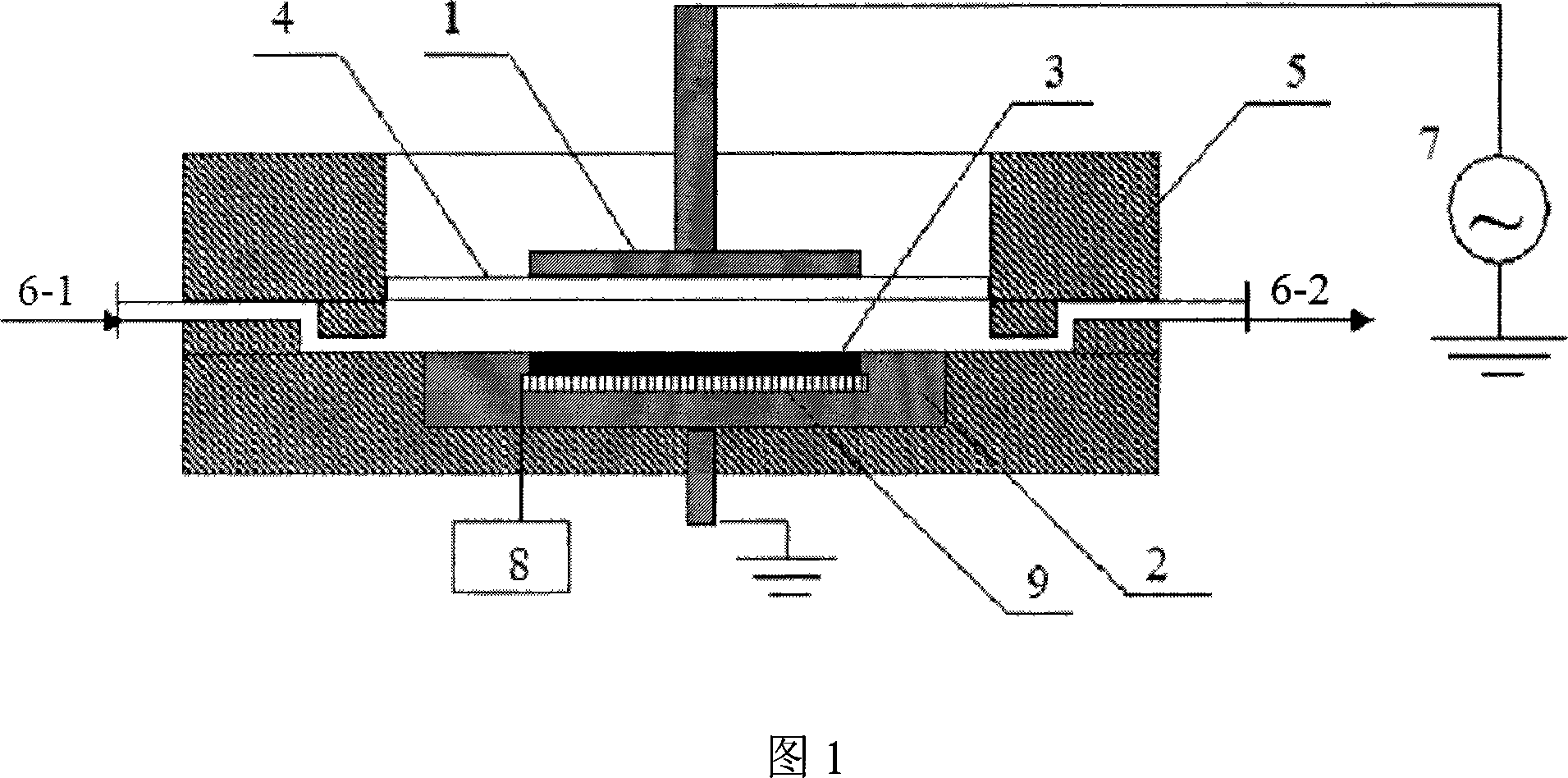
[0016] The glass substrate is cleaned on the surface, placed on the lower electrode of the reaction chamber, and the reaction chamber is evacuated to 10 -3 Pa, with pure nitrogen as the carrier gas, 20% silane (SiH 4 ) reaction gas, the pressure of the reaction chamber is 200Pa, the substrate is heated to 100°C, the high-voltage pulse power supply is turned on, the voltage is adjusted to 12KV, the frequency is 20KHz, the pulse rising edge is 20kV / μS, the pulse width is 2μS, and the film is deposited by gas discharge.

[0017] The amorphous hydrogen-silicon thin film prepared in this example has a uniform thickness and a firm bond with the film base. The maximum deposition rate of the film is 20nm / min according to the film thickness measurement by the step meter. According to the measurement and calculation of the ultraviolet-visible light transmission spectrum, its optical bandgap width is 1.92eV, which is larger than the optical bandgap (about 1.8eV) of the amorphous hydroge...

Embodiment 2

[0019] The aluminum plate is cleaned on the surface, placed on the lower electrode of the reaction chamber, and the reaction chamber is evacuated to 10 -3 Pa, with pure nitrogen as the carrier gas, 50% volume concentration of silane (SiH 4 ) reaction gas, the pressure of the reaction chamber is 100Pa, the substrate is heated to 50°C, the high-voltage pulse power supply is turned on, the voltage is adjusted to 20KV, the frequency is 10KHz, the rising edge of the pulse is 20kV / μS, the pulse width is 2μS, and the film is deposited by gas discharge.

[0020] The amorphous hydrogen-silicon thin film prepared in this example has a uniform thickness and a firm bond with the film base. The maximum deposition rate of the film is 15nm / min according to the film thickness measurement by the step meter. Analyzed by Raman spectroscopy, 480cm -1 The characteristic Raman peak of amorphous hydrogen-silicon appears at , which characterizes a typical amorphous hydrogen-silicon thin film.

Embodiment 3

[0022] The plastic substrate is cleaned on the surface, placed on the lower electrode of the reaction chamber, and the reaction chamber is evacuated to 10 -3 Pa, with pure nitrogen as the carrier gas, 40% silane (SiH 4 ) reaction gas, the reaction chamber pressure is 1000Pa, at room temperature, turn on the high-voltage pulse power supply, adjust the voltage 5KV, frequency 5KHz, pulse rising edge 20kV / μS, pulse width 2μS, gas discharge deposition film.

[0023] The amorphous hydrogen-silicon thin film prepared in this example has a uniform thickness and a firm bond with the film base. The maximum deposition rate of the film is 12nm / min according to the film thickness measurement by the step meter. Analyzed by Raman spectroscopy, 480cm -1 The characteristic Raman peak of amorphous hydrogen-silicon appears at , which characterizes a typical amorphous hydrogen-silicon thin film.


PUM

PropertyMeasurementUnit
thicknessaaaaaaaaaa
thicknessaaaaaaaaaa
optical band gapaaaaaaaaaa

Abstract

The present invention discloses process and apparatus for preparing amorphous hydrosilicon film. The process includes the steps of: setting cleaned substrate between two parallel electrodes inside a reaction chamber, vacuumizing the reaction chamber and filling pure nitrogen as carrier, introducing hydrogen diluted silane as the reacting gas, maintaining the substrate in room temperature or heating to 50-100 deg.c, and turning on the high voltage pulse power source for gaseous discharge to deposit film. The present invention realizes the fast deposition of amorphous hydrosilicon film on different kinds of substrate at room temperature or low temperature up to 50-100 deg.c in the maximum depositing rate up to 20 nm / min, 2 times higher than that of PECVD amorphous silicon film deposition. The prepared amorphous hydrosilicon film has energy gap of 1.92-2.18 eV, and may find its application in solar cell, energy saving building glass and other fields.

Description

technical field [0001] The invention relates to a method and a device for depositing amorphous hydrogen-silicon thin films on the surfaces of various substrates. Background technique [0002] Amorphous hydrogen silicon (a-Si:H) is a semiconductor thin film material that can achieve controllable doping. application. Most of the current a-Si:H film preparation methods follow the 1986 US patent: 4631198 (Kakinuma, et al.), using radio frequency discharge plasma chemical vapor deposition (PECVD) technology, using hydrogen and silane as reaction precursors, in Thin films are deposited on heated substrates. Atmospheric pressure chemical vapor deposition (APCVD) technology is also used to prepare amorphous silicon thin film transistors, which are applied to LCDs. See US Patent No. 5,930,657 (Kim, et al.) in 1999. So far, PECVD technology is still the commonly used preparation method for a-Si:H thin film research and large-scale industrial application. [0003] Conventional PECV...

Claims


Application Information

Patent Timeline
Patent Type & Authority Applications(China)
IPC IPC(8): C03C17/22C23C16/515C23C16/42C23C16/54
Inventor 张溪文李敏伟
Owner ZHEJIANG UNIV
Why Eureka
Try Eureka