
Manufacturing method and semiconductor element

Active Publication Date: 2021-07-15
NEC CORP
View PDF0 Cites 0 Cited by
  • Summary
  • Abstract
  • Description
  • Claims
  • Application Information

AI Technical Summary

Benefits of technology

The present patent describes a manufacturing method for a semiconductor element that controls the film thickness of the semiconductor layer accurately and easily. The method involves forming the element portion on a substrate portion through intermediation of a graphene layer at a monoatomic layer level and then removing the substrate portion by cleavage in the graphene layer. The graphene layer is soft, making the cleavage easy and minimizing the risk of damage to the element portion. The film thickness of the semiconductor layer can also be controlled accurately and easily. The method is secure in performance of the element portion and easy to remove the substrate portion and control the film thickness of the element portion.

Problems solved by technology

The semiconductor substrate causes incident light to attenuate, which may degrade detection sensitivity.
However, when mechanical polishing is used for removal of the substrate of the light receiving portion, a joint part of the light receiving portion and the element including the light receiving portion may be damaged.
Further, when chemical etching is used, it requires time to remove the entire substrate.
Specifically, removal of the semiconductor substrate used for forming the light receiving portion generally has a problem of degradation in element yield due to mechanical damage and complicated processing requiring increased time for assembling.

Method used


Image

  • Manufacturing method and semiconductor element
  • Manufacturing method and semiconductor element
  • Manufacturing method and semiconductor element

Examples


first example embodiment

[0053]The present example embodiment is an example embodiment relating to a semiconductor element, which is formed by, after forming the semiconductor element on a graphene layer formed on a semiconductor substrate, removing the semiconductor substrate by cutting off the semiconductor substrate from the graphene layer.

[Configuration and Operation]

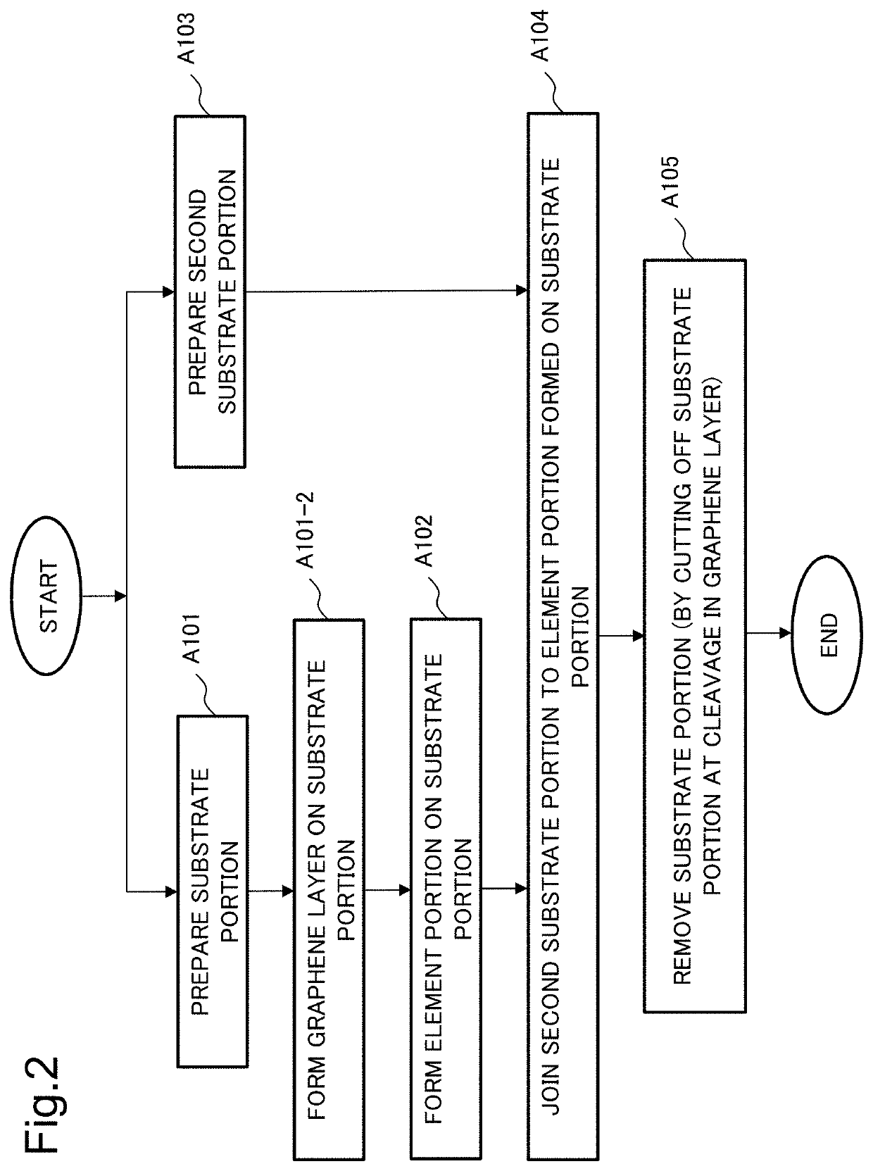
[0054]FIG. 2 is a schematic diagram illustrating a manufacturing method of a semiconductor element according to the present example embodiment.

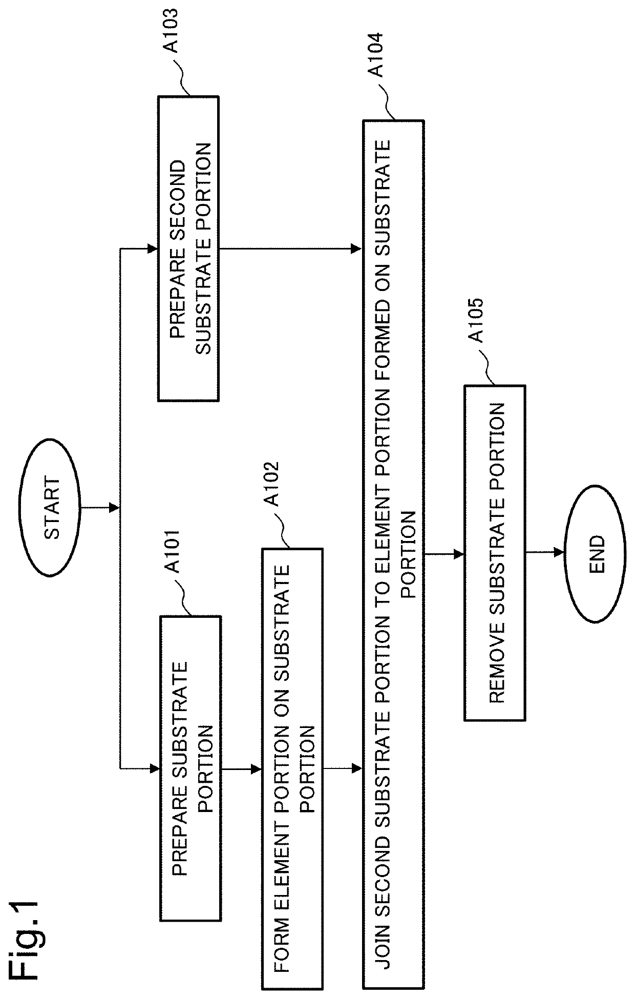
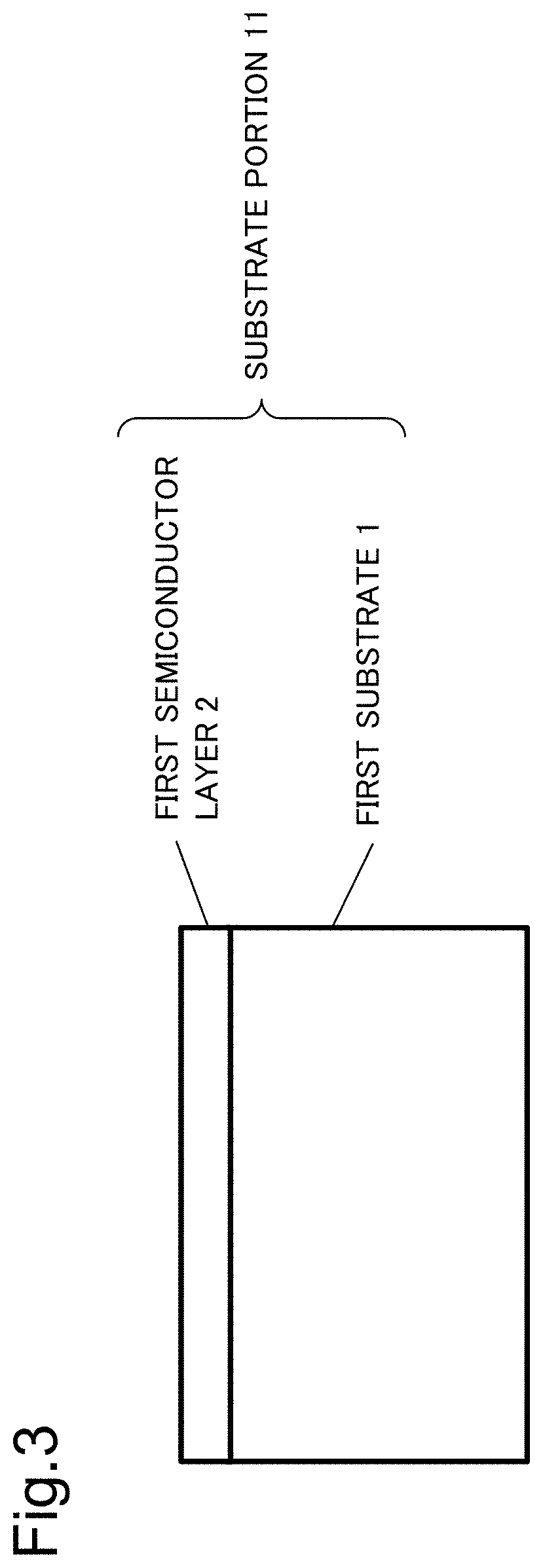
[0055]When operations in FIG. 2 are started, an operator or the like first prepares a substrate portion as an operation of A101. Herein, an operator or the like is an operator or a machine including a manufacturing robot for manufacturing a semiconductor element. The operation of A101 is equivalent to the operation of A101 in FIG. 1. A specific example of preparation for the substrate portion is described later with reference to FIG. 3.

[0056]Subsequently, as an operation of A101-2, an operator or the...

second example embodiment

[0090]The present example embodiment is an example embodiment relating to a manufacturing method in which a first recess is formed in a side portion directly on a graphene layer formed on a substrate portion and cleavage in the graphene layer is more facilitated.

[Configuration and Operation]

[0091]The manufacturing method according to the present example embodiment is illustrated in FIG. 2, and only the specific example of the operation of A102 in FIG. 2 is different. A part of the specific example of the operation of A102 in the present example embodiment, which is different from the first example embodiment, is mainly described below.

[0092]First, with reference to FIGS. 18 and. 19, the specific example of the operation of A102 in the present example embodiment is described.

[0093]When the operation of A102 in the present example embodiment is performed, an operator or the like first forms the configuration illustrated in FIG. 18. The configuration in FIG. 18 is different from the co...

third example embodiment

[0103]The present example embodiment is an example embodiment relating to a manufacturing method of a semiconductor element in which a recess is formed in a side portion of a semiconductor layer on a side of a substrate portion adjacent to a graphene layer for cleavage.

[Configuration and Operation]

[0104]The manufacturing method of a semiconductor element according to the present example embodiment is illustrated in FIG. 2, which is similar to the case in the second example embodiment, but the first recess formation layer 31 in FIGS. 18 to 21 is not present. In place of this, as illustrated in FIG. 22, a second recess formation layer 32 is inserted between the graphene layer 3 and the first semiconductor layer 2. The first recess formation layer 31 and the second recess formation layer 32 have similar structures and functions, but an insertion position differs.

[0105]The second recess formation layer 32 is formed of a material having a higher etching speed with respect to a predetermi...


PUM


Abstract

In order to enable simple removal of a substrate used for manufacturing a semiconductor element, a manufacturing method includes forming a graphene layer on a substrate portion formed of a semiconductor, forming an element portion on the graphene layer, the element portion including a semiconductor layer directly formed on the graphene layer, which takes over crystal information relating to the substrate portion when the semiconductor layer is formed on the substrate portion without intermediation of the graphene layer, and performing cutting-off between the substrate portion and the element portion at the graphene layer.

Description

[0001]This application is based upon and claims the benefit of priority from Japanese Patent Application No. 2020-004137, filed on Jan. 15, 2020, the disclosure of which is incorporated herein in its entirety by reference.TECHNICAL FIELD[0002]The present invention relates to a semiconductor element and a manufacturing method thereof.BACKGROUND ART[0003]In recent years, demands for high integration, size reduction, and high performance of electronic devices have been increased. In order to achieve those demands, there has been widely used a hybrid type semiconductor element employing flip-chip connection in which a semiconductor substrate is connected to another semiconductor substrate through intermediation of bump electrodes.[0004]As one example of such a hybrid type semiconductor element, PTL 1 discloses a hybrid type image sensor in which a light receiving portion and a circuit board are joined to each other. The hybrid type image sensor employs a structure in which the light rec...

Claims


Application Information

Patent Timeline
IPC IPC(8): H01L29/16H01L31/0352H01L29/04H01L21/02H01L31/18H01L27/146
CPCH01L29/1606H01L31/035272H01L27/146H01L21/02527H01L31/18H01L29/045H01L21/02425H01L21/0262H01L27/1469H01L31/1896H01L21/7806H01L21/02002
Inventor TANAKA, TOMO
Owner NEC CORP
Learn More