Wavelength Conversion Element and Method for Manufacturing Wavelength Conversion Element

a wavelength conversion element and wavelength conversion technology, applied in the field of optical devices, can solve the problems of difficult to obtain the desired waveguide structure, difficult to fabricate a nonlinear optical waveguide having specific desired nonlinear optical characteristics, and difficult to form an ln structure sized or shaped as designed, etc., to achieve the effect of low cost and efficient manufacturing

Active Publication Date: 2021-07-22
NIPPON TELEGRAPH & TELEPHONE CORP
View PDF0 Cites 1 Cited by
  • Summary
  • Abstract
  • Description
  • Claims
  • Application Information

AI Technical Summary

Benefits of technology

[0034]As described above, according to the present invention, a wave

Problems solved by technology

LN, which is a ferroelectric crystal, is a material that is hard to process, and it is difficult to form an LN structure sized or shaped as designed even if a semiconductor process capable of fine processing is used.
In the state of the art, considering also that the nonlinear optical effect in the PPLN waveguide using the quasi-phase matc

Method used


Image

  • Wavelength Conversion Element and Method for Manufacturing Wavelength Conversion Element
  • Wavelength Conversion Element and Method for Manufacturing Wavelength Conversion Element
  • Wavelength Conversion Element and Method for Manufacturing Wavelength Conversion Element

Examples


first embodiment

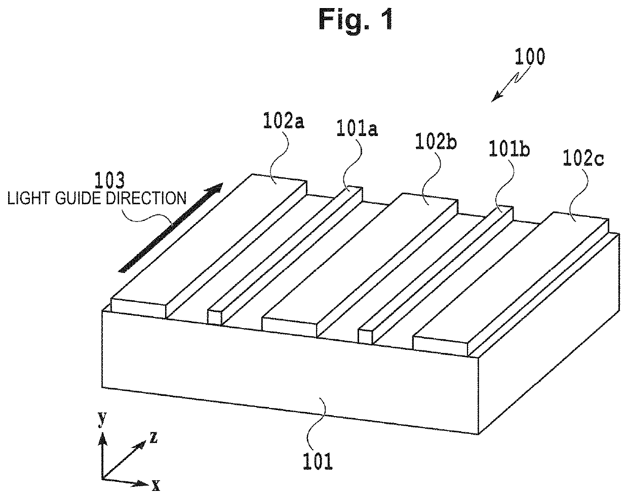
[0047]FIG. 4 is a conceptual diagram for illustrating a configuration of a wavelength conversion device according to a first embodiment of the present invention. The configuration corresponds to the configuration of the conventional wavelength conversion device shown in FIG. 1. A wavelength conversion device 400 in FIG. 4 is a chip including a plurality of waveguides cut from a substrate in which a large number of waveguides (arrayed waveguides) is formed. The wavelength conversion device 400 includes a plurality of waveguides 401a and 401b and slab waveguides 402a to 402c that are formed substantially in parallel with and spaced apart from the plurality of waveguides. All the waveguides are formed along a z-axis direction, and light can be input to and output from the wavelength conversion device 400 at two end faces (x-y faces) defining the outer shape of the chip of the wavelength conversion device 400 that are perpendicular to the waveguides (z-axis) and oriented in the depth di...

second embodiment

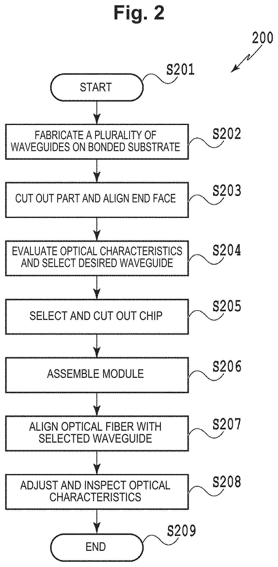
[0061]In steps for fabricating the wavelength conversion device, arrayed waveguide having cores reduced in size to increase the wavelength conversion efficiency are fabricated. At this point, slab waveguides are formed as a result of the problems of the dry etching being solved. With the wavelength conversion device according to the first embodiment described above, in order to efficiently perform the step of selecting one waveguide having desired characteristics from a plurality of waveguides, guided light attenuators are formed in the slab waveguides. With regard to a wavelength conversion device according to a second embodiment, a configuration and a method for more efficiently performing a step of mounting the wavelength conversion device in a module after selecting a desired waveguide and then performing an adjustment and an inspection of the wavelength conversion device will be described.

[0062]As shown in FIG. 2, in order to use the wavelength conversion device in practice, a ...

example 1

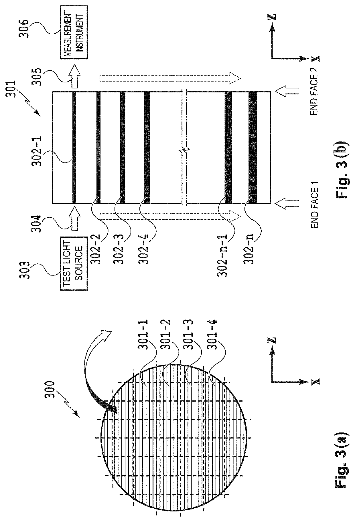
[0074]Referring to FIG. 6 again, FIG. 6 is a top view of the wavelength conversion device 600 in an example 1. The waveguides 601-1 to 601-n for wavelength conversion are made of a ferroelectric primarily made up of lithium niobate whose spontaneous polarization is periodically inverted. A lower substrate constituting a cladding portion is made of lithium tantalite having a coefficient of thermal expansion close to that of lithium niobate. The material forming the waveguides 601-1 to 601-n is a nonlinear optical material. The material forming the substrate constituting the cladding or an over-cladding may be any material that is transparent to the light in the two wavelength bands used for wavelength conversion, such as a dielectric material or semiconductor material, such as silicon, silicon dioxide, lithium niobate, indium phosphide, or polymers, or a compound of such a dielectric material or semiconductor material and an additive. The two wavelength bands can be a band around 155...


PUM


Abstract

With a wavelength conversion device based on a nonlinear optical effect, when arrayed waveguides including an intended nonlinear waveguide are fabricated, unwanted slab waveguides are inevitably formed. The slab waveguides can cause an erroneous measurement in the selection of a waveguide having desired characteristics from the arrayed waveguides. The erroneous measurement can lead to redoing steps for fabricating the wavelength conversion device and a decrease in the yield and inhibit the evaluation of the characteristics in selection of the waveguide and the subsequent fabrication of the wavelength conversion device from being efficiently performed. A wavelength conversion device according to the present invention includes a plurality of waveguides formed on a substrate, and a plurality of slab waveguides that are arranged substantially in parallel with and spaced apart from the plurality of waveguides, and a guided light attenuator is formed in each of the slab waveguides. The guided light attenuators allow efficient selection of a waveguide having desired optical characteristics from the plurality of waveguides. The light attenuation by the guided light attenuators can be changed in steps for fabricating the wavelength conversion device.

Description

TECHNICAL FIELD[0001]The present invention relates to an optical device based on a nonlinear optical effect. More specifically, the present invention relates to a wavelength conversion device used for an optical communication system or optical measurement system, for example.BACKGROUND ART[0002]Optical application technologies based on nonlinear optical effects are expected to find uses in fields such as optical communication or optical quantum information communication. A known one of basic nonlinear optical effects is wavelength conversion, which converts light incident on a nonlinear optical medium into light of a different frequency. More specifically, a technique is widely known which uses the characteristics of the wavelength conversion to generate light in a wavelength band that is hardly oscillated by a laser by itself. In particular, a periodically poled lithium niobate (PPLN) waveguide made of lithium niobate (LiNbO3), which is a second-order nonlinear material and has a h...

Claims


Application Information

Patent Timeline
IPC IPC(8): G02B6/122G02B6/13G02F1/377
CPCG02B6/122G02B2006/1204G02F1/377G02B6/13G02B2006/12126G02B2006/12045G02B6/12011
Inventor KASHIWAZAKI, TAKAHIROKASAHARA, RYOICHITADANAGA, OSAMUUMEKI, TAKESHIEMBUTSU, KOJIKAZAMA, TAKUSHI
Owner NIPPON TELEGRAPH & TELEPHONE CORP
Why Eureka
Try Eureka