Supercharge Your Innovation With Domain-Expert AI Agents!

Embedded PHY (EPHY) IP Core for FPGA

a technology of embedded physical layer and gate array, which is applied in the direction of generating/distributing signals, instruments, computation using non-denominational number representation, etc., can solve the problems of increasing the total system bill of materials (bom) cost, insufficient testing and validation of devices that require low-speed phys, and external low-speed phy chips

Active Publication Date: 2021-09-02
WESTERN DIGITAL TECH INC
View PDF4 Cites 1 Cited by
  • Summary
  • Abstract
  • Description
  • Claims
  • Application Information

AI Technical Summary

Benefits of technology

The present patent is about an embedded physical layer (EPHY) that is used for a field programmable gate array (FPGA). This EPHY can be used for testing devices or any application that needs to implement MIPI PHY, such as data storage / memory applications, display applications, communication applications, and more. The use of this EPHY allows for flexibility and supporting any specification updates without the need for ASIC production cycles.

Problems solved by technology

The typical FPGA, due to the presence of high speed PHYs, are unable to adequately test and validate the devices that require low speed PHYs.
There are many problems with using an external low speed PHY chip.
Using a large amount of signals forces the testing device FPGA to have a large input / output (I / O) count that increases the total system bill of materials (BOM) cost.
Also, an external testing PHY chip on a shuttle application specific integrated circuit (ASIC) has a substantial cost of a few hundred US dollars per chip.
Additionally, scalability for the next generation of devices is a concern because the interface is limited on I / O counts at speed, and therefore the next speed for the next generation of devices will need to double the speed on the I / F or double the I / O, both of which are not feasible.
Finally, to gain time and be the first device in the market, relying on the ASIC PHY design and waiting for the next test chip (for the next generation speed) to be developed depends upon the timing of the ASIC PHY release and thus does is naturally delayed.
The capabilities are thus limited since the testing device does not see the I / F to a device under testing (DUT).
Due to the limitation, mimicking other devices for testing is limited, as is validation of DUTs.
Hence, using an external PHY device to implement MPHY, which is the current solution for UFS testing devices, is not optimal.
An ASIC tape out will cost millions of US dollars for a prototype shuttle.

Method used


Image

  • Embedded PHY (EPHY) IP Core for FPGA
  • Embedded PHY (EPHY) IP Core for FPGA
  • Embedded PHY (EPHY) IP Core for FPGA

Examples


Embodiment Construction

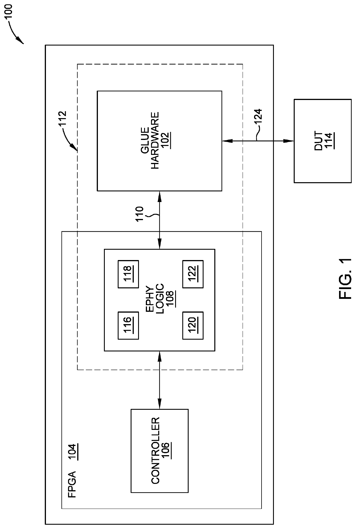
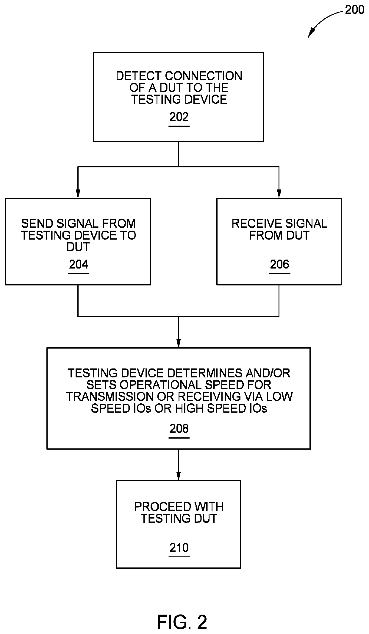
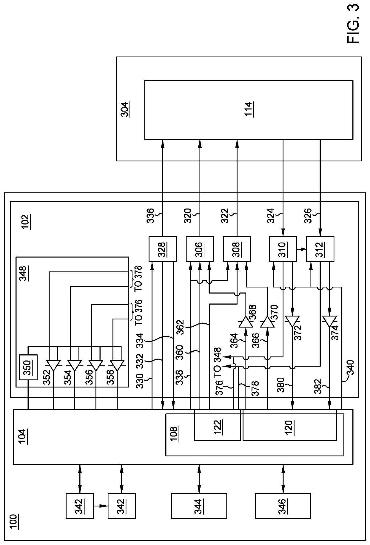
[0017]In the following, reference is made to embodiments of the disclosure. However, it should be understood that the disclosure is not limited to specific described embodiments. Instead, any combination of the following features and elements, whether related to different embodiments or not, is contemplated to implement and practice the disclosure. Furthermore, although embodiments of the disclosure may achieve advantages over other possible solutions and / or over the prior art, whether or not a particular advantage is achieved by a given embodiment is not limiting of the disclosure. Thus, the following aspects, features, embodiments and advantages are merely illustrative and are not considered elements or limitations of the appended claims except where explicitly recited in a claim(s). Likewise, reference to “the disclosure” shall not be construed as a generalization of any inventive subject matter disclosed herein and shall not be considered to be an element or limitation of the ap...


PUM


Abstract

The present disclosure generally relates to an embedded physical layer (EPHY) for a field programmable gate array (FPGA). The EPHY for the FPGA is for a testing device that can receive and transmit in both the high speed PHYs, as well as low speed PHYs, such as MIPI PHYs (MPHYs), to meet universal flash storage (UFS) specifications. The testing device with the EPHY for the FPGA provides flexibility to support any specification updates without the need of application specific (ASIC) production cycles.

Description

BACKGROUND OF THE DISCLOSUREField of the Disclosure[0001]Embodiments of the present disclosure generally relate to an embedded physical layer (EPHY) for a field programmable gate array (FPGA).Description of the Related Art[0002]As devices are developed, they need to be validated with a testing device. Typical testing devices include an FPGA that has high speed physical layers (PHYs). Many devices to be tested require low speed PHYs, such as the Mobile Industry Processor Interface (MIPI) PHYs (MPHY), interfaces to meet universal flash storage (UFS) specifications. The typical FPGA, due to the presence of high speed PHYs, are unable to adequately test and validate the devices that require low speed PHYs. In order to adequately test and validate the devices, an external low speed PHY chip is used to align the low speed PHYs with the high speed PHYs.[0003]There are many problems with using an external low speed PHY chip. For example, the MPHY to unified protocol (UNIPRO) MAC interface (...

Claims


Application Information

Patent Timeline
IPC IPC(8): G01R31/3183G01R31/00G06F30/347G06F7/64G06F1/04
CPCG01R31/318335G01R31/002G06F1/04G06F7/64G06F30/347G01R31/31917G01R31/31908
Inventor GANON, DORONLERNER, EITAN
Owner WESTERN DIGITAL TECH INC
Features
  • R&D
  • Intellectual Property
  • Life Sciences
  • Materials
  • Tech Scout
  • Unparalleled Data Quality
  • Higher Quality Content
  • 60% Fewer Hallucinations
Learn More