Unlock instant, AI-driven research and patent intelligence for your innovation.

Array substrate and method of preparing the same

Active Publication Date: 2021-09-16
WUHAN CHINA STAR OPTOELECTRONICS SEMICON DISPLAY TECH CO LTD
View PDF0 Cites 0 Cited by
  • Summary
  • Abstract
  • Description
  • Claims
  • Application Information

AI Technical Summary

Benefits of technology

The present patent aims to provide an array substrate and a method of preparing the same, which involves forming an oxide layer on the sidewalls of the active layer and the crystallization layer to obstruct the source / drain metal layer from contacting the active layer, thereby reducing the likelihood of leakage current. This technique achieves the purpose of reducing the leakage current and ensuring the stability and reliability of the array substrate.

Problems solved by technology

However, excimer laser annealing (ELA) technology is adopted in conventional LTPS production for crystallization, in which machines are expensive and production cost is high.
Moreover, a case of uneven brightness is easily generated during crystallization by the ELA technology due to poor uniformity, so that large-sized display panels cannot be produced.

Method used


Image

  • Array substrate and method of preparing the same
  • Array substrate and method of preparing the same

Examples


Embodiment Construction

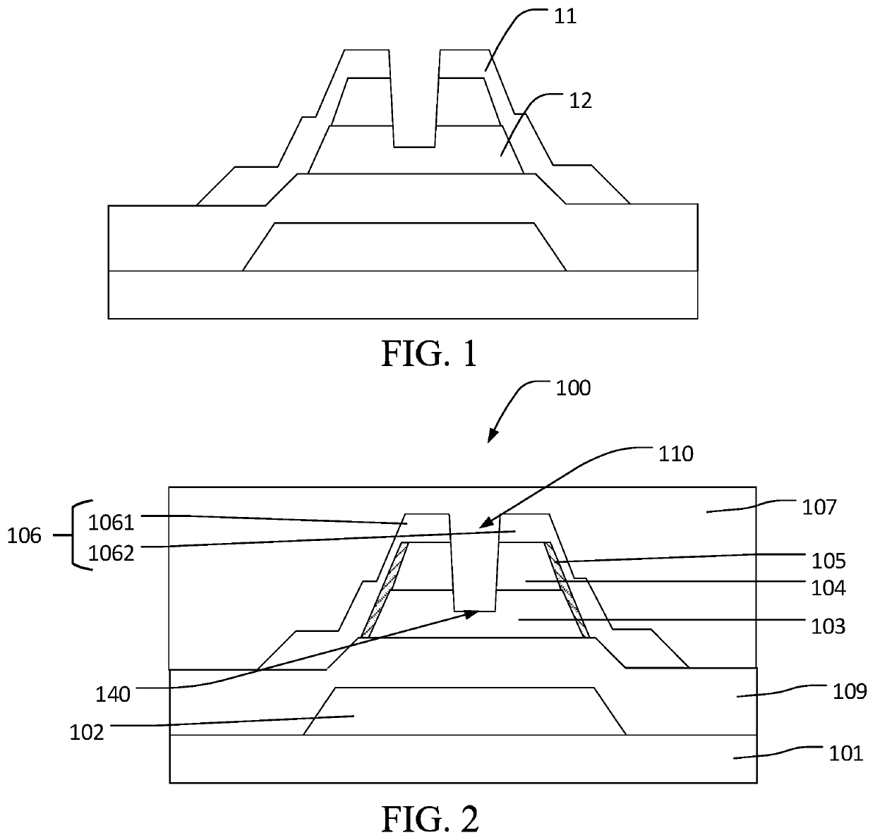
[0028]A description of each embodiment with reference to accompanying drawings is as follows to illustrate specific embodiments in which the present disclosure can be implemented. Directional terms mentioned in the present disclosure, such as “up”, “down”, “front”, “back”, “left”, “right”, “inner”, “outer”, and “side”, are only used for directions referring to the drawings. Names of components mentioned in the present disclosure, such as “first” and “second”, are only used to distinguish different components, which can be better expressed. In the drawings, similarly structural units are indicated by the same reference numerals.

[0029]Embodiments of the present disclosure will be described in detail herein with reference to the accompanying drawings. The disclosure may be implemented in many different forms and should not be construed as being limited to specific embodiments set forth herein. The embodiments of the present disclosure are provided to explain the practical application o...


PUM


Abstract

The present disclosure provides an array substrate and a method of preparing the same. The array substrate includes a substrate, a gate, a gate insulation layer, an active layer, a crystallization layer, an oxide layer, a source / drain metal layer, and a passivation layer. After the crystallization layer is prepared, a mask plate is not removed and is used to protect an upper surface of the crystallization layer from oxidation reaction. Then, an oxide layer is formed on sidewalls of the crystallization layer and the active layer. The oxide layer is used to obstruct the source / drain metal layer from contacting the active layer. The source / drain metal layer is only in contact with the crystallization layer, thereby reducing a path of leakage current and achieving a purpose of reducing the leakage current.

Description

FIELD OF THE INVENTION[0001]The present disclosure relates to the technical field of displays, and specifically to an array substrate and a method of preparing the same.BACKGROUND OF THE INVENTION[0002]Low temperature poly-silicon (LTPS) technology has advantages, such as high electron mobility, better sub-threshold swing, large on / off states current ratio, low power consumption, high pixel density, and being able to apply to flexible organic light-emitting diode (OLED) substrates, and has attracted widespread attention in recent years. However, excimer laser annealing (ELA) technology is adopted in conventional LTPS production for crystallization, in which machines are expensive and production cost is high. Moreover, a case of uneven brightness is easily generated during crystallization by the ELA technology due to poor uniformity, so that large-sized display panels cannot be produced. In addition, since solid phase crystallization (SPC) technology has advantages, such as low cost ...

Claims


Application Information

Patent Timeline
IPC IPC(8): H01L29/786H01L29/45H01L29/66H01L21/02
CPCH01L29/78678H01L21/02667H01L29/66765H01L29/458H01L27/1222H01L27/127H01L29/0653H01L29/0638H01L29/78609
Inventor FAN, CHENGJUN
Owner WUHAN CHINA STAR OPTOELECTRONICS SEMICON DISPLAY TECH CO LTD