Thin film forming device and thin film forming method using the same

Pending Publication Date: 2021-09-23
JUSUNG ENG
View PDF0 Cites 1 Cited by
  • Summary
  • Abstract
  • Description
  • Claims
  • Application Information

AI Technical Summary

Benefits of technology

The patent is about a device and method for making silicon thin films with improved quality. By dividing the reaction space in the device and using plasma treatment in a separate space, impurities in the silicon film can be removed and the grain sizes of the crystals can be made uniform, resulting in a high-quality film with excellent properties.

Problems solved by technology

However, in a substrate which is formed with a pattern, as a line width of the pattern narrows and an aspect ratio increases, it is difficult to form or grow a uniform silicon thin film on the pattern.
As such, as a line width of the pattern narrows and an aspect ratio increases, it is difficult to form or grow a silicon thin film having a uniform or appropriate step coverage on the top, side and bottom of the pattern, by a thin film forming method generally known in the conventional art.
Also, it is substantially difficult to uniformly remove impurities in the silicon thin film formed on the top, side and bottom of the pattern.

Method used


Image

  • Thin film forming device and thin film forming method using the same
  • Thin film forming device and thin film forming method using the same
  • Thin film forming device and thin film forming method using the same

Examples


Embodiment Construction

[0026]Hereinafter, various embodiments will be described in detail with reference to the accompanying drawings to the extent that a person skilled in the art to which the embodiments pertain may easily enforce the embodiments. Among the reference numerals presented in the drawings, like reference numerals denote like members.

[0027]In describing the present disclosure, when it is determined that the detailed description of the known related art may obscure the gist of the present disclosure, the detailed description thereof will be omitted.

[0028]Although the terms such as first and second may be used to describe various components, the components are not limited by the terms, and the terms are used only to distinguish components from other components.

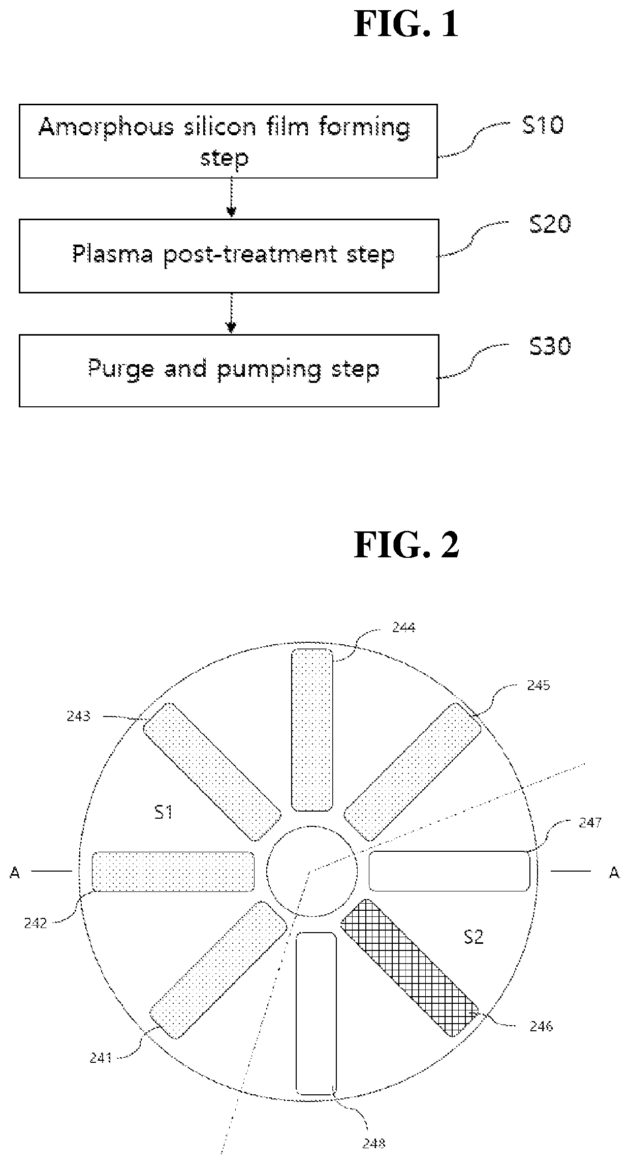
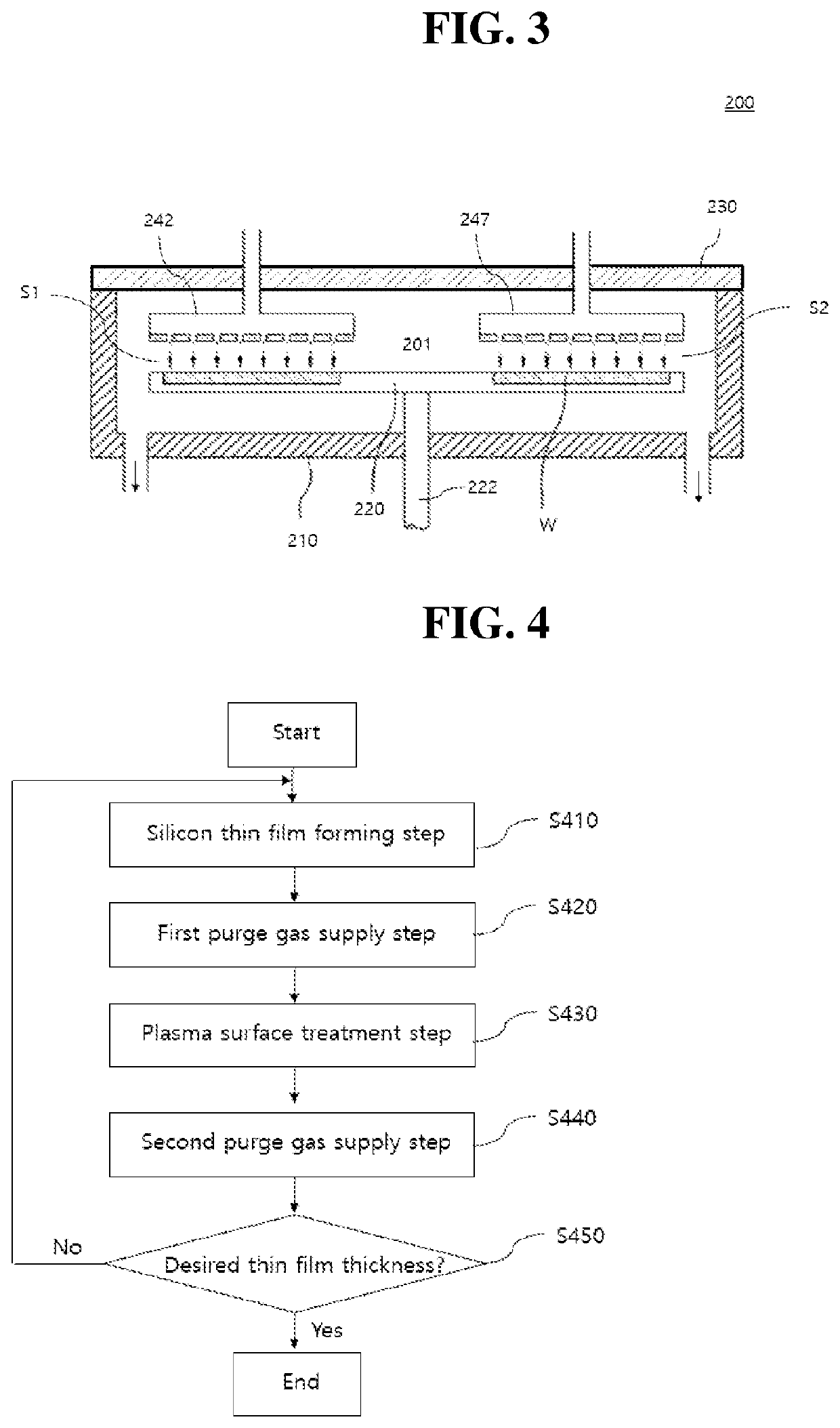
[0029]FIG. 2 is a representation of an example of a view to assist in the explanation of a planar structure in a chamber of a thin film forming device in accordance with an embodiment of the disclosure, and FIG. 3 is a sectional view tak...


PUM

PropertyMeasurementUnit
Grain sizeaaaaaaaaaa
Timeaaaaaaaaaa
Thicknessaaaaaaaaaa

Abstract

The disclosure relates to a thin film forming device and a thin film forming method using the same capable of improving the film quality of a silicon thin film by dividing a reaction space in a process chamber of the thin film forming device and thereby forming the silicon thin film on a substrate in a first space and treating a surface of the silicon thin film, formed in the first space, in a second space by using plasma. By the thin film forming device and the thin film forming method using the same according to the disclosure, with a trend that a pattern is complicated and the depth of the pattern increases, impurities in a thin film may be more efficiently removed, a uniform thin film may be formed on a pattern, and the grain size of the crystals of a silicon thin film may be made uniform.

Description

BACKGROUND1. Technical Field[0001]Various embodiments generally relate to a thin film forming device and a thin film forming method using the same, and more particularly, to a thin film forming device and a thin film forming method using the same capable of improving the film quality of a silicon thin film by dividing a reaction space in a process chamber of the thin film forming device and thereby forming the silicon thin film on a substrate in a first space and treating a surface of the silicon thin film, formed in the first space, in a second space by using plasma.2. Related Art[0002]In general, in order to form a thin film having a predetermined thickness on a substrate such as a semiconductor wafer, a glass or the like, thin film forming methods employing physical vapor deposition (PVD) using physical collisions such as sputtering, chemical vapor deposition (CVD) using chemical reactions, atomic layer deposition (ALD), and so forth are used.[0003]As the CVD, atmospheric pressur...

Claims


Application Information

Patent Timeline
IPC IPC(8): H01L21/02H01L21/66H01J37/32C23C16/455C23C16/50C23C16/458C23C16/24C23C16/52
CPCH01L21/0262H01L21/02592H01L21/02598H01L21/02532H01L21/02661H01L22/26H01J2237/332C23C16/45536C23C16/50C23C16/4584C23C16/24C23C16/52H01J37/3244H01L21/67H01L21/02C23C16/45551C23C16/45534C23C16/45519
Inventor KOO, BUN HEIHWANG, CHUL-JOO
Owner JUSUNG ENG
Why Eureka
Try Eureka