
Circuitry for transferring data across reset domains

a technology of reset domains and circuits, applied in the direction of electric digital data processing, instruments, generating/distributing signals, etc., can solve the problems of metastability at a destination register in the second reset domain, the reset path is often untimed, and the multi-domain device can be troublesome to opera

Active Publication Date: 2021-10-28
NORDIC SEMICONDUCTOR
View PDF0 Cites 0 Cited by
  • Summary
  • Abstract
  • Description
  • Claims
  • Application Information

AI Technical Summary

Benefits of technology

The patent describes a circuit that ensures reliable data transfer between two registers. It includes a reset detector that checks if a reset has occurred in a first register. If a reset is detected, the circuit allows the data to be read from the buffer and ensures that only reliable data passes through. This prevents metastability issues that can occur when data is transferred between registers. The circuit also includes synchronizers that help avoid metastability in logic gates within the circuit. Overall, this circuit improves the accuracy and reliability of data transfer between registers.

Problems solved by technology

Reset paths are often untimed—i.e. they not synchronized to a clock signal that is also provided to the components.
A problem can arise in a multi-domain device if data is crossing from a first reset domain to a second reset domain—e.g. over a data bus from a slave MCU to a master MCU—around the time the first reset domain is reset, but where the second reset domain is not reset.
The resetting of the first reset domain may result in metastability at a destination register in the second reset domain.
This metastability can lead to data corruption in the destination register, resulting in unpredictable or erroneous behaviour of the device.
However, such clock gating is not always desirable as it can prevent processes in the destination reset domain from executing in a timely manner.

Method used


Image

  • Circuitry for transferring data across reset domains
  • Circuitry for transferring data across reset domains
  • Circuitry for transferring data across reset domains

Examples


Embodiment Construction

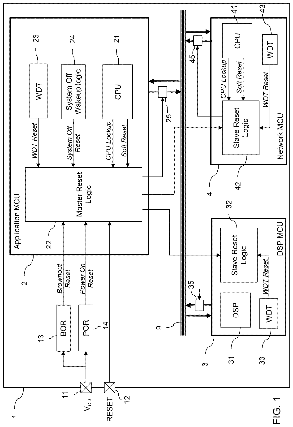
[0040]FIG. 1 shows elements of an integrated-circuit system-on-chip (SoC) 1 that embodies the invention.

[0041]The SoC 1 comprises an application micro-controller unit (MCU) 2, a digital signal processing (DSP) MCU 3, and a Network MCU 4. The Network MCU 4 could, for example, include a radio transceiver such as a Bluetooth Low Energy™ radio. The Application MCU 2 contains a CPU 21 for executing a main software application. The Network MCU also contains its own CPU 31 for executing network communication libraries. The DSP MCU 3 contains a DSP 31 for performing intensive calculations such as floating-point arithmetic. The MCUs 2, 3, 4 can exchange data with each other, and with a non-volatile memory (not shown), over a bus system 9.

[0042]Other standard components of an SoC such as volatile and non-volatile memory, peripherals, interfaces, power management, clock management, etc. are omitted from FIG. 1 for simplicity but may be present in the SoC 1. Instead, FIG. 1 focuses in particula...


PUM


Abstract

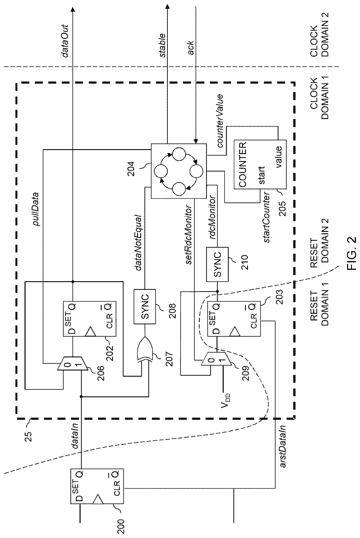
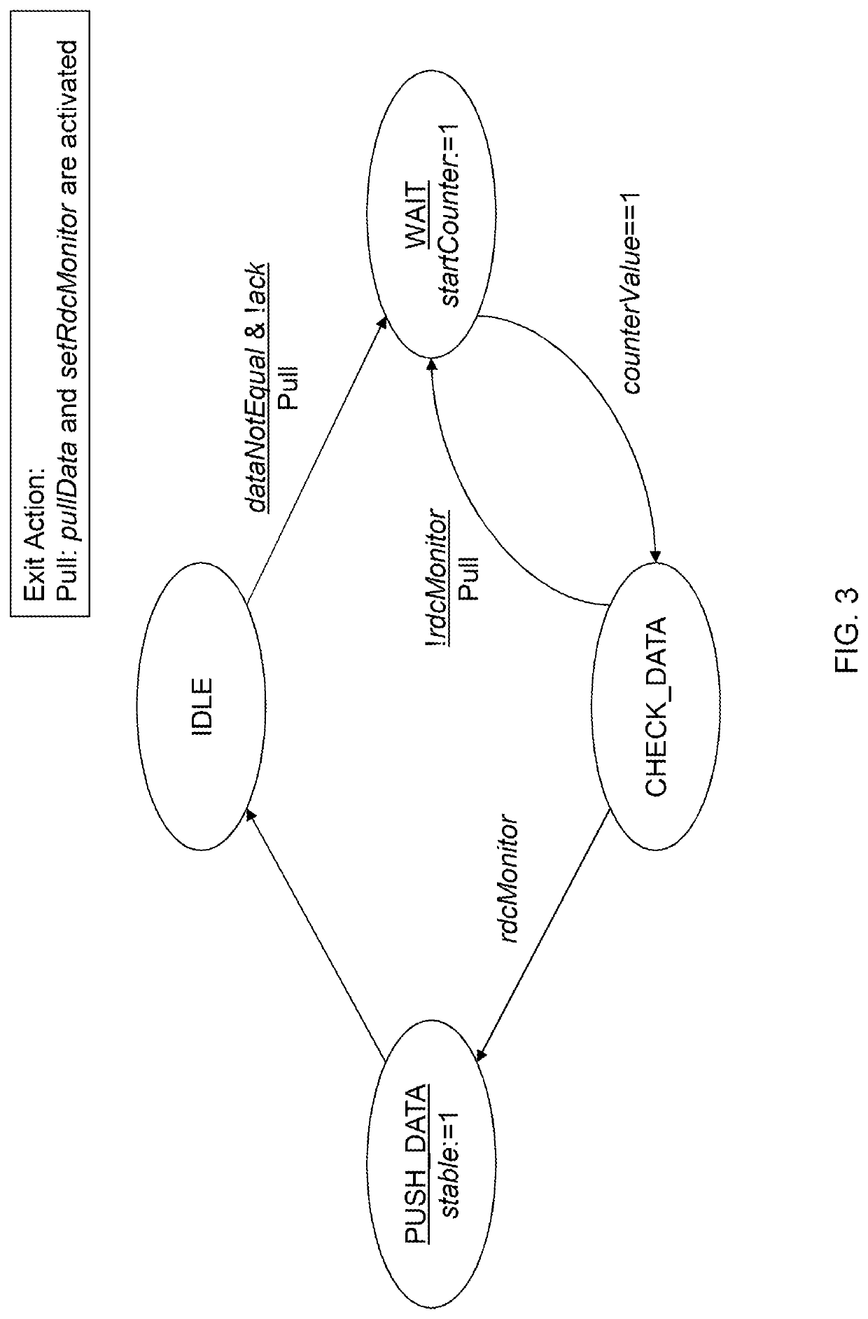
An integrated-circuit device comprises a source register in a reset domain, a destination circuit outside the reset domain, and a reset checking circuit. The checking circuit comprises a buffer outside the reset domain for receiving data values output by the source register, a reset detector, and reset checking logic. The checking logic detects a new data value output by the source register, checks whether a reset of the reset domain has been detected, and contingently outputs a control signal for controlling whether the destination circuit receives the new data value from the buffer. The reset detector signals whether a reset has been detected by using a feedback path to hold a predetermined value in a resettable latch until the latch receives a reset signal, and to hold a different value in the latch after receiving a reset signal.

Description

CROSS-REFERENCE TO RELATED APPLICATION[0001]This application claims priority from United Kingdom Patent Application No. GB2005960.6, filed Apr. 23, 2020, which application is incorporated herein by reference in its entirety.BACKGROUND OF THE INVENTION[0002]This invention relates to integrated-circuit devices comprising circuitry for transferring data across reset domains.[0003]Many integrated-circuit (IC) devices, such as microcontrollers, are configured to reset to a known state under particular conditions. These conditions may include: if a processor encounters an illegal instruction; once the supply voltage has stabilised at power on (a “power-on reset”); upon detecting a power brown-out; if a watchdog timer triggers due to a lockup on the device; or when an external reset pin is asserted (e.g. by a user pressing a physical reset button of an apparatus that incorporates the IC device).[0004]Reset logic on the device may issue a reset signal to components (e.g. D-type flip-flops) ...

Claims


Application Information

Patent Timeline
IPC IPC(8): G06F1/24G06F1/12G06F13/40G06F1/08
CPCG06F1/24G06F1/08G06F13/4054G06F1/12
Inventor OJA, ARIHOLEN, ÅSMUNDVENÅS, ARNE WANVIKAUSTBØ, KNUTHAUGEN, RAGNAR
Owner NORDIC SEMICONDUCTOR
Learn More