
Dark-field optical inspecting device

a technology of optical inspection and dark field, applied in the direction of optically investigating flaws/contamination, measurement devices, instruments, etc., can solve the problems of photometric loss corresponding to the radiation portion, scratching, surface roughness, etc., and achieve the effect of very efficient collection

Pending Publication Date: 2021-11-11
UNITY SEMICON
View PDF3 Cites 0 Cited by
  • Summary
  • Abstract
  • Description
  • Claims
  • Application Information

AI Technical Summary

Benefits of technology

This patent describes a way to collect different parts of light that are spread over a wide area. The light is reflected and directed to specific devices that collect each part of the light. This results in efficient and effective collection of the light.

Problems solved by technology

Defects can be crystal defects, scratches, asperities, or surface roughness.
Therefore, this approach discriminates the diffuse radiation according to the azimuthal angle over a wide spatial area, which necessarily leads to a photometric loss corresponding to the portion of the radiation that is not collected by the fibers or the pixels.
The azimuthal angle distribution information is therefore obtained at the cost of a loss of signal, which can lead to imposing a relatively long acquisition time and hence to a relatively low inspection rate.
What is more, the spatial resolving of this light spot brings an increased risk of crosstalk at the transitions between the zones to be distinguished.

Method used


Image

  • Dark-field optical inspecting device
  • Dark-field optical inspecting device
  • Dark-field optical inspecting device

Examples


Embodiment Construction

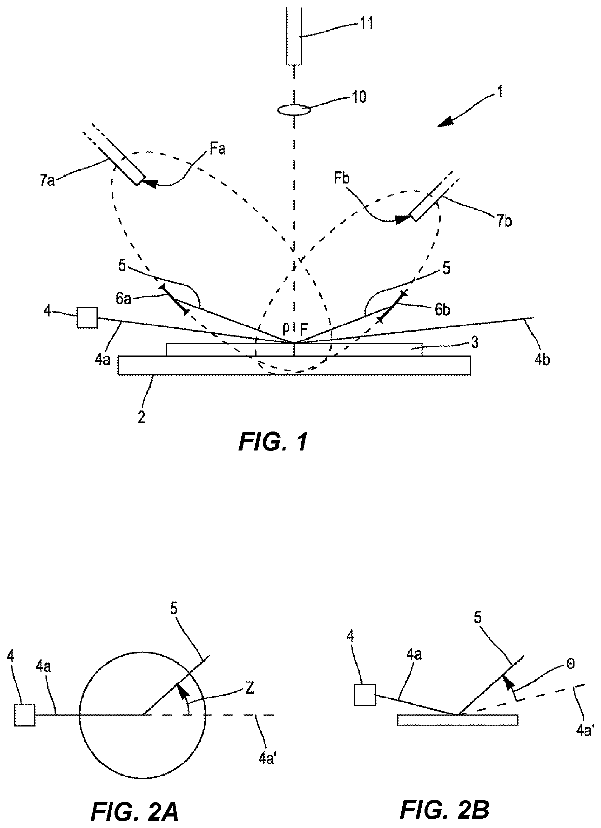
[0040]FIG. 1 shows a schematic of a dark-field optical inspection device 1 according to the present description. A chamber defines an internal space that is isolated from the exterior light. The internal space comprises a support 2 for a substrate 3.

[0041]The substrate 3 can, for example, be or comprise a wafer made of a semiconductor material such as silicon or germanium, or an insulating material such as glass, or it can even be composed of a plurality of layers, and it can be bare or provided with electronic or optical circuits described above, for example. The substrate 3 can, for example, also comprise any type of substrate that is known in the semiconductor industry, MEMS, or integrated optics, such as “wafers on frame,”“dicing frames,” or “panels”, for example.

[0042]The support 2 can be set in motion or caused to rotate or move translationally, for example, in a direction that is included in the plane defined by the support so as to enable the entire exposed surface of the su...


PUM

PropertyMeasurementUnit
angleaaaaaaaaaa
angleaaaaaaaaaa
azimuth angleaaaaaaaaaa

Abstract

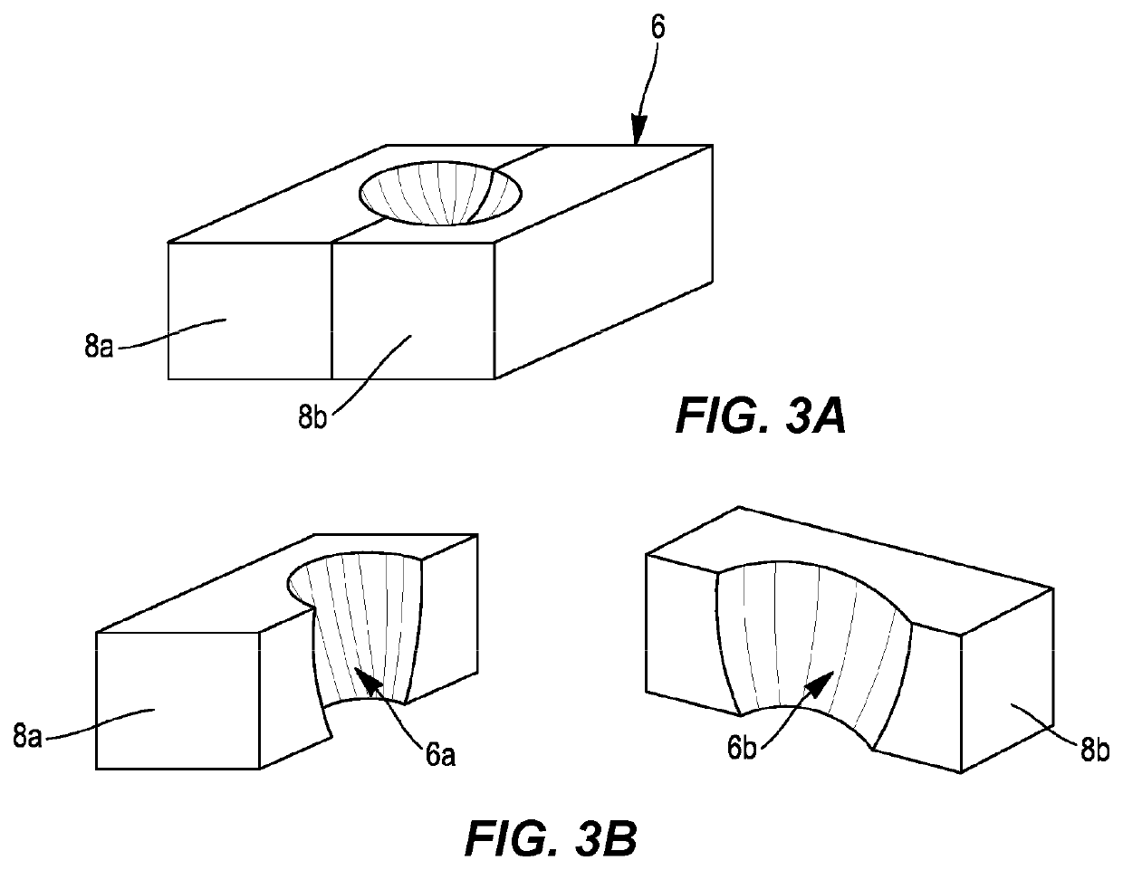
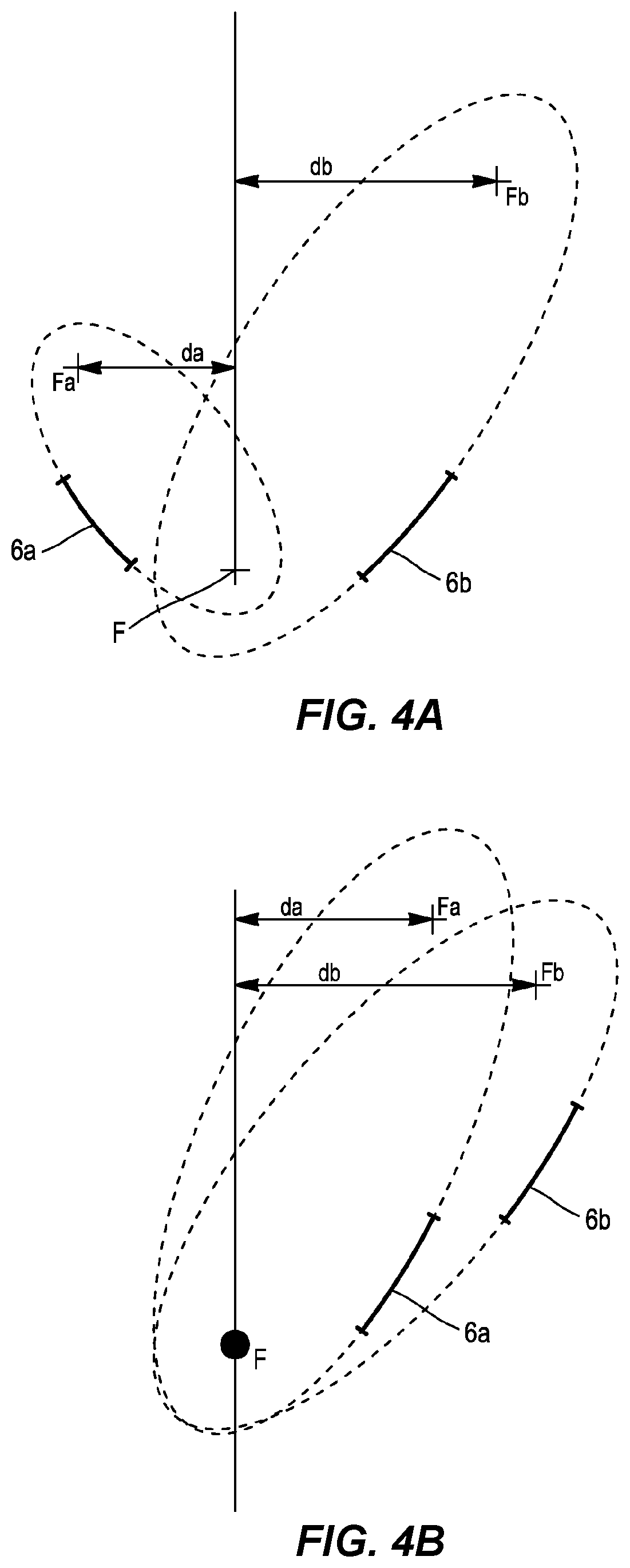
A device for dark-field optical inspection of a substrate comprises: a light source for generating an incident beam that is projected onto an inspection zone of the substrate and that is capable of being reflected in the form of diffuse radiation; at least one first and one second collecting device; and a reflecting device for directing at least a portion of the diffuse radiation originating from a focal point of collection coincident with the inspection zone in the direction of the collecting devices, with a first and second reflective zone from which a first portion of the diffuse radiation is directed toward a first focal point, which is optically conjugated with the focal point of collection, and a second portion of the diffuse radiation is reflected toward a second focal point, which is optically conjugated with the collection focal point and distinct from the first focal point of detection.

Description

CROSS-REFERENCE TO RELATED APPLICATIONS[0001]This application is a national phase entry under 35 U.S.C. § 371 of International Patent Application PCT / FR2019 / 052210, filed Sep. 20, 2019, designating the United States of America and published as International Patent Publication WO 2020 / 074800 A1 on Apr. 16, 2020, which claims the benefit under Article 8 of the Patent Cooperation Treaty to French Patent Application Serial No. 1859311, filed Oct. 8, 2018.TECHNICAL FIELD[0002]The present disclosure relates to a device for dark-field optical inspection of a substrate in order to detect therein the possible presence of a defect or of a particle, or more generally to characterize the surface condition thereof. The substrate can be a wafer for manufacturing components in the field of electronics, optics, or optoelectronics.BACKGROUND[0003]Substrates, such as wafers, for electronics, optics or optoelectronics must be inspected in order to be able to detect, identify, and / or characterize any d...

Claims


Application Information

Patent Timeline
Patent Type & Authority Applications(United States)
IPC IPC(8): G01N21/88G01N21/95G01N21/47
CPCG01N21/8806G01N21/9501G01N21/9506G01N2021/4742G01N2021/8822G01N2021/4709G01N2021/4707G01N21/474G01N2021/4704
Inventor DURAND DE GEVIGNEY, MAYEUL
Owner UNITY SEMICON
Learn More