Semiconductor package

Active Publication Date: 2021-11-11
MITSUBISHI ELECTRIC CORP
View PDF0 Cites 2 Cited by
  • Summary
  • Abstract
  • Description
  • Claims
  • Application Information

AI Technical Summary

Benefits of technology

[0003]In a transfer-molded power module, a power device operating at a high voltage is mounted on a lead frame. When the spacer and the power device are adjacent to each other, insulation performance lowers due to an insufficient cree

Problems solved by technology

When the spacer and the power device are adjacent to each other, insulation performance lowers due to an insufficient creepage distance.
Further, there has been a problem that the power module may be used under a severe condition such as a high temperature condition, the package is subjected to a stress, the spacer is thus damaged, and reliability lowers.
However

Method used


Image

  • Semiconductor package
  • Semiconductor package
  • Semiconductor package

Examples


first embodiment

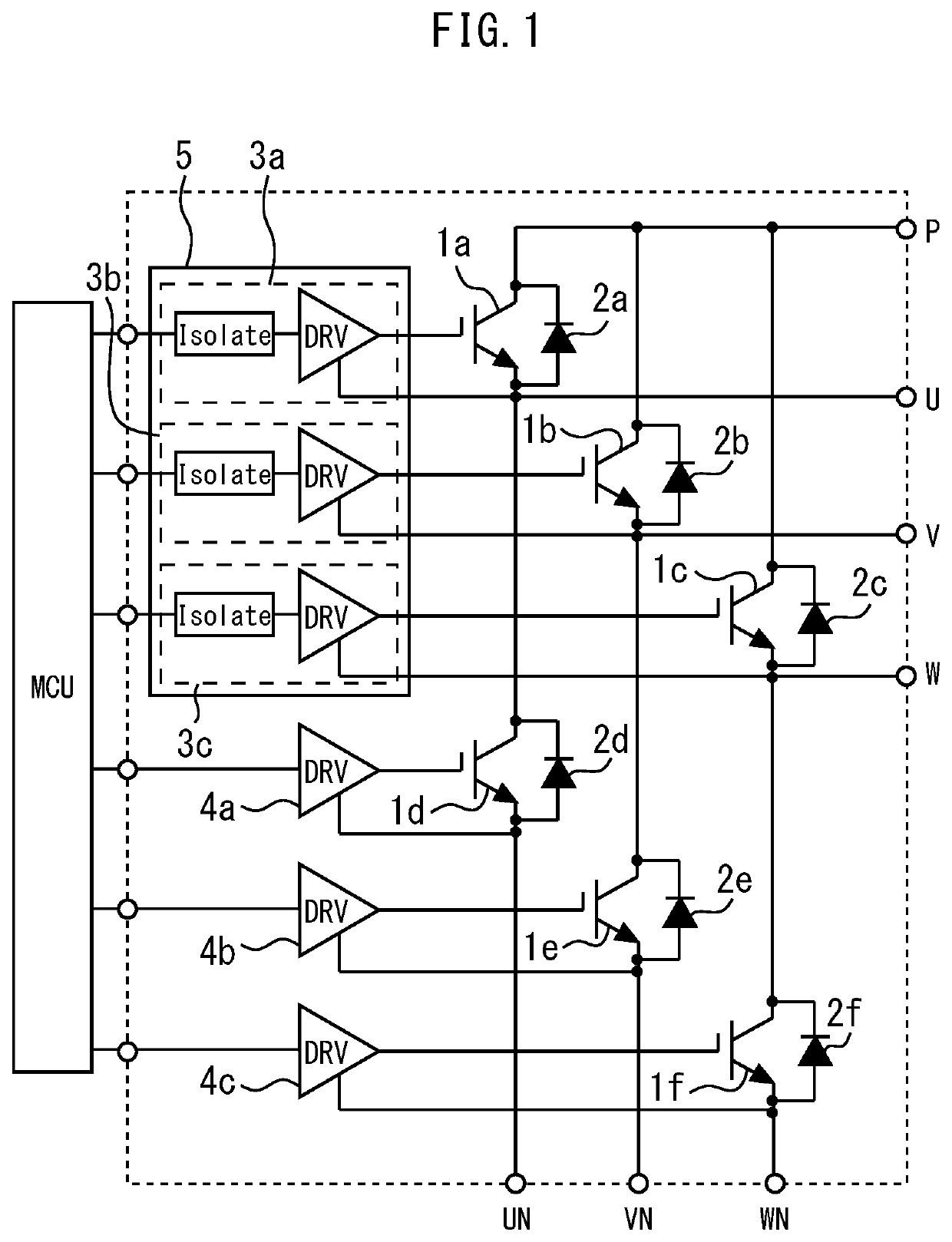
[0019]FIG. 1 is a circuit diagram of a semiconductor package according to a first embodiment. This semiconductor package is a transfer-molded power module. P-side semiconductor devices 1a, 1b, and 1c and N-side semiconductor devices 1d, 1e, and 1f are IGBTs and are switching devices of three-phase inverters. Diodes 2a to 2f are freewheeling diodes and are respectively connected in anti-parallel with the semiconductor devices 1a to 1f.

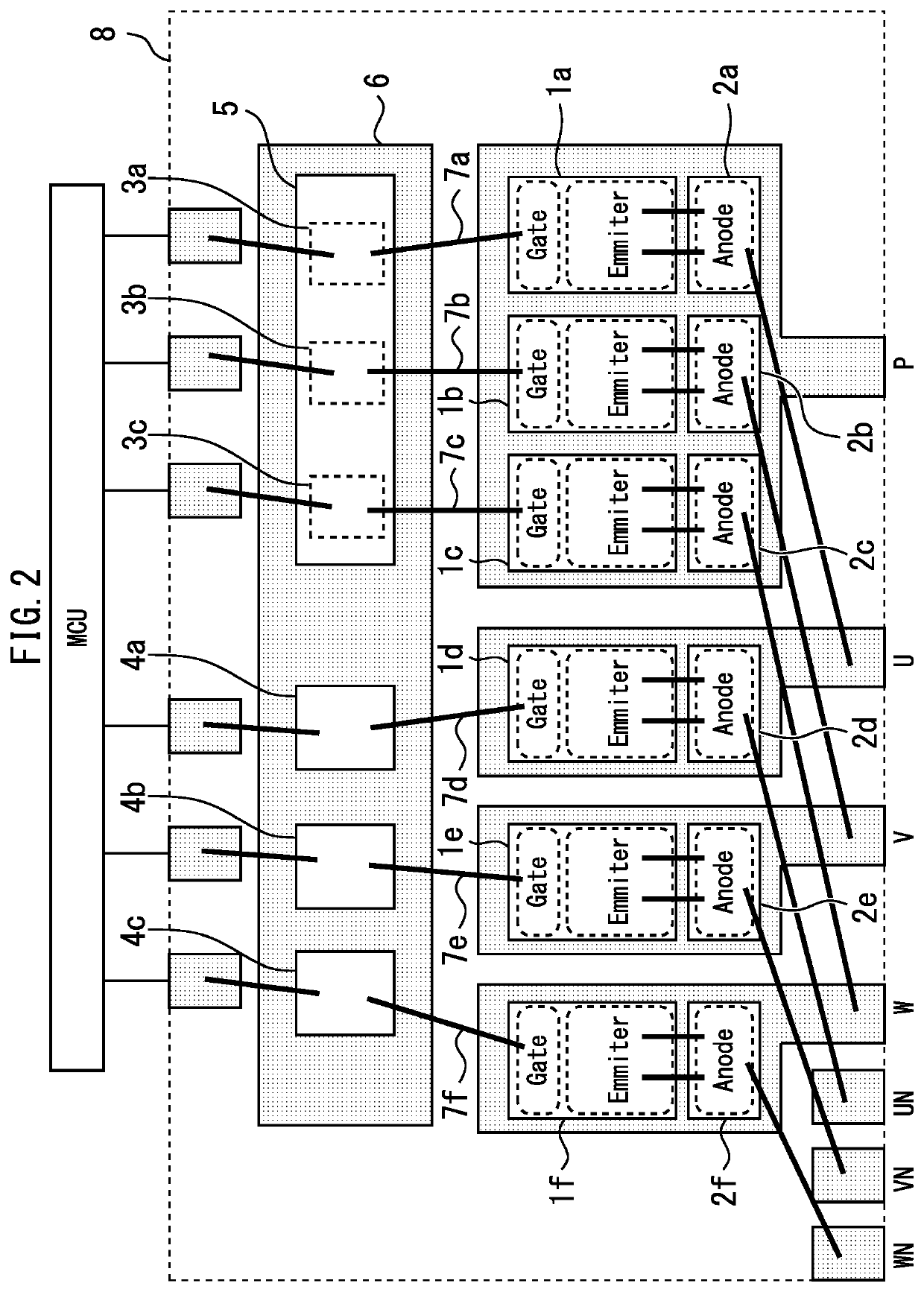
[0020]Three high-voltage-side insulated drivers 3a, 3b, and 3c respectively drive the P-side semiconductor devices 1a, 1b, and 1c of three phases in accordance with an input signal from a micro-controller unit (MCU). Three low-voltage-side drivers 4a, 4b, and 4c respectively drive the N-side semiconductor devices 1d, 1e, and 1f of three phases in accordance with an input signal. The three high-voltage-side insulated drivers 3a, 3b, and 3c are integrated in one built-in package 5.

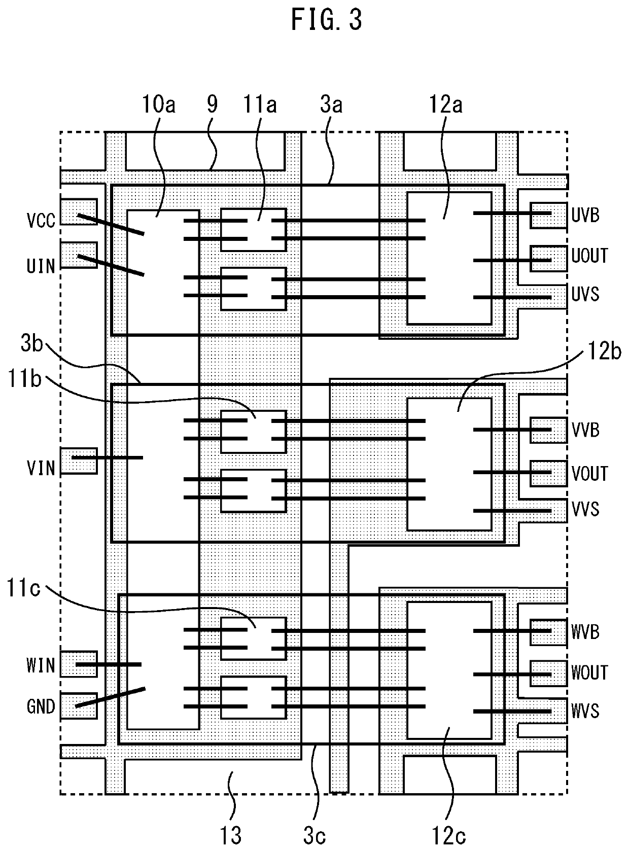
[0021]FIG. 2 is a plan view illustrating an internal portion of the semico...

second embodiment

[0033]FIG. 6 is a circuit diagram of a semiconductor package according to a second embodiment. FIG. 7 is a plan view illustrating an internal portion of the semiconductor package according to the second embodiment. Similarly to the first embodiment, the three high-voltage-side insulated drivers 3a, 3b, and 3c are integrated in one built-in package 5. Here, depending on the usage, in order to remove an influence due to noise between a semiconductor module and a system of a client, there is a case where a signal isolator may be needed for a low-voltage-side driver. Accordingly, in this embodiment, low-voltage-side insulated drivers 3d, 3e, and 3f are used as low-voltage-side drivers driving the N-side semiconductor devices 1d, 1e, and 1f of three phases. Further, similarly to the high-voltage-side insulated drivers 3a, 3b, and 3c of the first embodiment, the three low-voltage-side insulated drivers 3d, 3e, and 3f are integrated in one built-in package 15. Accordingly, signal isolation...

third embodiment

[0034]FIG. 8 is a circuit diagram of a semiconductor package according to a third embodiment. FIG. 9 is a plan view illustrating an internal portion of the semiconductor package according to the third embodiment. The three high-voltage-side insulated drivers 3a, 3b, and 3c and the three low-voltage-side insulated drivers 3d, 3e, and 3f, which correspond to a total of six phases on the P side and N side, are integrated in one built-in package 16. Accordingly, the size of an apparatus may be reduced, and wiring may be reduced. The other configurations and effects are similar to the second embodiment.

[0035]The semiconductor devices 1a to 1f are not limited to semiconductor devices formed of silicon, but instead may be formed of a wide-bandgap semiconductor having a bandgap wider than that of silicon. The wide-bandgap semiconductor is, for example, a silicon carbide, a gallium-nitride-based material, or diamond. A semiconductor device formed of such a wide-bandgap semiconductor has a hi...


PUM


Abstract

A semiconductor package includes: a semiconductor device; a lead frame; a built-in package including an insulated driver having a multi-chip configuration and driving the semiconductor device; a wire connecting the built-in package to the semiconductor device; and a resin sealing the semiconductor device, the lead frame, the built-in package, and the wire, wherein the built-in package is directly joined to the lead frame.

Description

BACKGROUND OF THE INVENTIONField[0001]The present disclosure relates to a semiconductor package.Background[0002]For a transfer-molded power module, package in package (PIP) is used in which another built-in package is sealed in a transfer-molded package. In related art, a built-in package is installed in a substrate while being supported by a spacer or the like, and the whole package is sealed by a resin (for example, see paragraph 0062 and FIG. 2 of JP 2008-198907 A).SUMMARY[0003]In a transfer-molded power module, a power device operating at a high voltage is mounted on a lead frame. When the spacer and the power device are adjacent to each other, insulation performance lowers due to an insufficient creepage distance. Further, there has been a problem that the power module may be used under a severe condition such as a high temperature condition, the package is subjected to a stress, the spacer is thus damaged, and reliability lowers.[0004]Further, a high-voltage-side driving unit ...

Claims


Application Information

Patent Timeline
IPC IPC(8): H01L23/495H01L23/00H01L23/31
CPCH01L23/49575H01L24/45H01L23/3107H01L23/49503H01L23/4952H01L23/49562H01L2924/1426H01L2224/48245H01L2224/48699H01L2924/10272H01L2924/1033H01L2924/13055H01L2224/48137H01L25/18H01L2224/49175H01L2224/48091H01L2224/45124H01L2224/45144H01L2224/45139H01L2224/48247H01L2924/19107H01L2924/181H01L2224/0603H01L24/49H01L24/48H01L2224/29101H01L2224/83801H01L24/29H01L24/83H01L2224/73265H01L2224/32245H01L24/32H01L2224/48257H01L2924/00014H01L2924/00012H01L2924/00H01L2924/014
Inventor IMANISHI, MOTOKI
Owner MITSUBISHI ELECTRIC CORP
Why Eureka
Try Eureka