

Laminated semiconductor ceramic capacitor with varistor function and method for manufacturing the same
a technology of laminated semiconductor ceramic capacitors and varistor functions, which is applied in the direction of fixed capacitors, stacked capacitors, fixed capacitor details, etc., can solve the problems of reducing apparent relative permittivity rapp /sub>or the insulation resistance, affecting the performance of grain boundary insulating layers, and affecting the performance of insulating layers. , to achieve the effect of suppressing variations in characteristics, good apparent relative permittivity rapp, and good
- Summary
- Abstract
- Description
- Claims
- Application Information
AI Technical Summary
Benefits of technology
Problems solved by technology
Method used
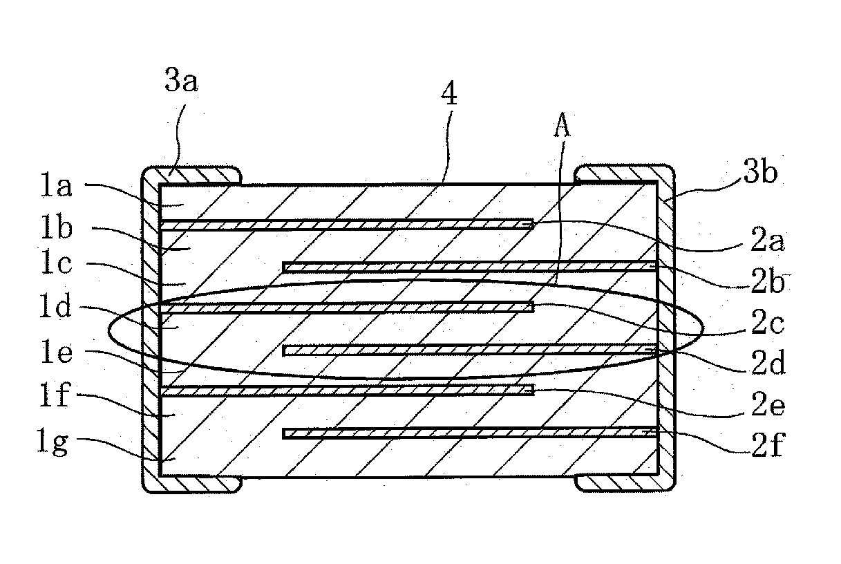
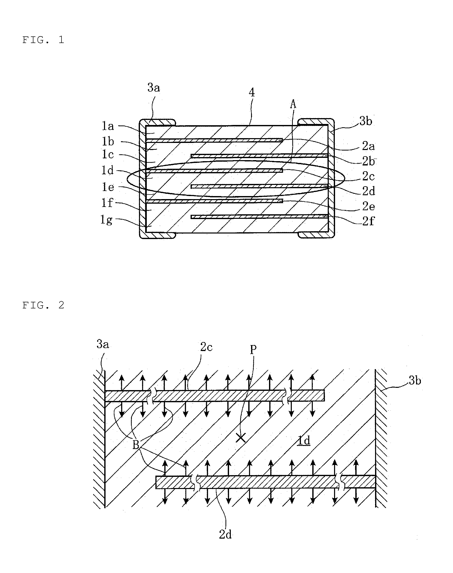
Image

Examples
example 1
Preparation of Samples
[0108]As ceramic raw materials, SrCO3, TiO2 having a specific surface area of 30 m2 / g (average grain diameter: about 30 nm), and LaCl3 as a donor compound were prepared. Then, LaCl3 was weighed in such a way that the content of La was 0.8 mol with respect to 100 mol of the Ti element, and further SrO3 and TiO2 were weighed in such a way that the compounding molar ratio m of a Sr site to a Ti site (=Sr site / Ti site) was set as shown in Table 1.
[0109]Then, 3 parts by weight of ammonium polycarboxylate were added as a dispersant to 100 parts by weight of these weighed materials, and then the resulting mixture was charged into a ball mill with PSZ balls of 2 mm in diameter as a pulverizing medium and pure water, and subjected to wet mixing for 16 hours in the ball mill to prepare a slurry.
[0110]Next, this slurry was evaporated to dryness, and then subjected to a calcination treatment at a calcining temperature shown in Table 1 for 2 hours in an atmosphere of the ai...
example 2
[0136]A ceramic slurry was prepared by the same method / procedure as in the example 1 except that the compounding molar ratio m of a Sr site to a Ti site was 1.000, the molar content of Mn was 0.3 mol with respect to 100 mol of the Ti element, and the molar content of SiO2 was 0.1 mol with respect to 100 mol of the Ti element. In addition, the calcining treatment was performed at a calcining temperature shown in Table 2.
[0137]Next, using a lip coater method, the ceramic slurry was subjected to forming process and a ceramic green sheet was prepared so as to have a thickness of a semiconductor ceramic layer of a value shown in Table 2 after firing. Then, a conductive paste for internal electrodes predominantly composed of Ni was used to be applied onto the ceramic green sheet by screen printing, thereby forming a conductive film with a predetermined pattern on the surface of the ceramic green sheet.
[0138]Then, the effective number shown in Table 2 of ceramic green sheets having the con...
PUM
| Property | Measurement | Unit |
|---|---|---|
| average grain diameter | aaaaa | aaaaa |
| average grain diameter | aaaaa | aaaaa |
| thickness | aaaaa | aaaaa |
Abstract
Description
Claims
Application Information