Unlock instant, AI-driven research and patent intelligence for your innovation.

Integration of an active component on a photonics platform

a photonics platform and active component technology, applied in the field of photonics, can solve the problems of inability to monolithically obtain optical components such as infrared light sources on silicon platforms, inability to achieve monolithic acquisition of optical components, etc., and achieve the effect of improving alignmen

Pending Publication Date: 2022-03-10
INDIGO DIABETES NV
View PDF0 Cites 3 Cited by
  • Summary
  • Abstract
  • Description
  • Claims
  • Application Information

AI Technical Summary

Benefits of technology

The present invention allows for very precise control over the size and layers of the active component, as well as the depth of the recess. This can improve alignment between the active component and the waveguide in the waveguide layer. The recess can be created by etching or grinding into the photonics substrate. The active component is placed in the recess and fixed in position using glue or other suitable methods. The active component can be a radiation source and the method can involve fixing the position of the active component and then detecting a radiation signal and adjusting the placement of the active component accordingly.

Problems solved by technology

However, some optical components, such as infrared light sources, cannot be monolithically obtained in a silicon platform, because they have an inherently poor energy efficiency.
Photodetectors have been recently realized in a CMOS process flow, but they have some limitation on the cut-off wavelengths.
Similarly, it is not possible to monolithically fabricate electro-optics components (like switches, modulators, etc.) in a silicon nitride (SiN) platform because it responds poorly to electrical signals.
One of the major difficulties occurring in these integration techniques relates to obtaining a good alignment accuracy of the active component onto the photonic structures.
Usually, an accuracy of circa 1 μm or better is required, especially when the component is the light source: even a micron-size misalignment can cause losses because light needs to be coupled to a mode size structure.
However, these supports, or optical benches are typically bulky.
If horizontal light coupling is required, for instance if the light source bandwidth is too wide for a grating coupler, the flip-chip approach is not applicable.
Several alternative approaches have been attempted to achieve accurate alignment, but they have been proven unpractical and require additional alignment tweaking after component placement.
Transfer-printing has been proposed recently which allows horizontal coupling and compact integration, but alignment reproducibility is poor because it relies on a shear-driven component release process using a PDMS stamp.
In addition, the process is heavily material dependent.
For example, printing III-V components involves a certain level of mechanical stress intrinsic to the process, that may result in structural material defects, such as dislocations that may later reduce the quality of the epitaxial layers in the light source.
This quality reduction may cause current leakage, lower efficiency, etc.
In reality, this requires a separate dedicated facility since commercial CMOS facilities never allow gold in the fab because it kills the performance of the CMOS circuit components.
The latter makes electrical connectivity still time consuming and vulnerable.

Method used


Image

  • Integration of an active component on a photonics platform
  • Integration of an active component on a photonics platform
  • Integration of an active component on a photonics platform

Examples


Embodiment Construction

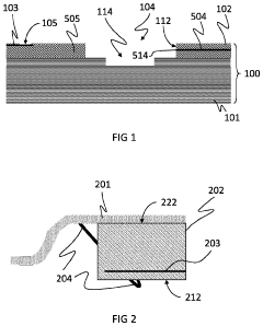
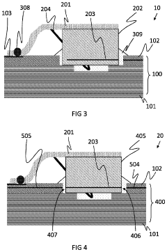
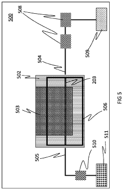
[0063]The present invention will be described with respect to particular embodiments and with reference to certain drawings, but the invention is not limited thereto but only by the claims. The dimensions and the relative dimensions do not correspond to actual reductions to practice of the invention.

[0064]Furthermore, the terms first, second and the like in the description and in the claims, are used for distinguishing between similar elements and not necessarily for describing a sequence, either temporally, spatially, in ranking or in any other manner. It is to be understood that the terms so used are interchangeable under appropriate circumstances and that the embodiments of the invention described herein are capable of operation in other sequences than described or illustrated herein.

[0065]Moreover, the terms top, under and the like in the description and the claims are used for descriptive purposes and not necessarily for describing relative positions. It is to be understood tha...


PUM


Abstract

A photonics integrated circuit includes a photonics platform having a waveguide layer having a waveguide and a wiring substrate with an active component positioned thereon and extending therefrom. The active component has a component top surface facing away from the wiring substrate and component side surfaces through which radiation can be coupled. The photonics platform comprises a recess wherein the active component can be positioned such that the component top surface of the active component is positioned on a surface of the recess. The photonics platform and the active component are being configured for allowing lateral optical coupling between the waveguide in the photonics platform and at least one of the component side surfaces of the active component.

Description

FIELD OF THE INVENTION[0001]The invention relates to the field of photonics. More specifically it relates to integration and coupling of active components, such as for example light sources, in photonics platforms.BACKGROUND OF THE INVENTION[0002]Optical platforms for transmission of optical signals can be used for a variety of applications such as sensing, information communication, signal conversion, and are applied in different fields such as telecommunications, health applications. A number of photonic platforms have been developed in recent decades, of which silicon based photonic platforms are the most popular.[0003]However, some optical components, such as infrared light sources, cannot be monolithically obtained in a silicon platform, because they have an inherently poor energy efficiency. Photodetectors have been recently realized in a CMOS process flow, but they have some limitation on the cut-off wavelengths. Similarly, it is not possible to monolithically fabricate elect...

Claims


Application Information

Patent Timeline
IPC IPC(8): G02B6/12G02B6/13
CPCG02B6/12004G02B6/13G02B6/12G02B6/136G02B6/42G02B6/422G02B6/4225G02B6/43
Inventor CARDILE, PAOLOVAN SCHUYLENBERGH, KOENRAADVAN ACOLEYEN, KARELDELBEKE, DANAE
Owner INDIGO DIABETES NV