Neutral atom imaging unit, neutral atom imager, neutral atom imaging method, and space detection system

a technology of neutron atom and imaging method, applied in the field of neutron atom imaging, can solve the problems of unremitting efforts of space community, biggest obstacle to reliable ena measurements, and inability to develop space neutron atom detection technology, etc., to achieve good spatial resolution, time resolution and energy resolution, and better imaging

Active Publication Date: 2022-03-24
PEKING UNIV
View PDF1 Cites 0 Cited by
  • Summary
  • Abstract
  • Description
  • Claims
  • Application Information

AI Technical Summary

Benefits of technology

[0054]3. The neutral atom imager of the present disclosure may include nearly one thousand semiconductor detectors, with the detection area reaching 200 cm2 and the geometrical factor reaching 13.3 cm2sr. Therefore, the neutral atom imager of the present disclosure has good spatial resolution, time

Problems solved by technology

However, the development of space neutral atom detection technology has not been easy.
The extremely strong extreme ultraviolet/ultraviolet radiation (EUV/UV) background existing in the space is the biggest obstacle to reliable ENA measurements.
The space community has made unremitting efforts in the field of space neutral atom detection technology.
However, due to the extremely strong extreme ultraviolet/ultraviolet radiati

Method used


Image

  • Neutral atom imaging unit, neutral atom imager, neutral atom imaging method, and space detection system
  • Neutral atom imaging unit, neutral atom imager, neutral atom imaging method, and space detection system
  • Neutral atom imaging unit, neutral atom imager, neutral atom imaging method, and space detection system

Examples


embodiment 1

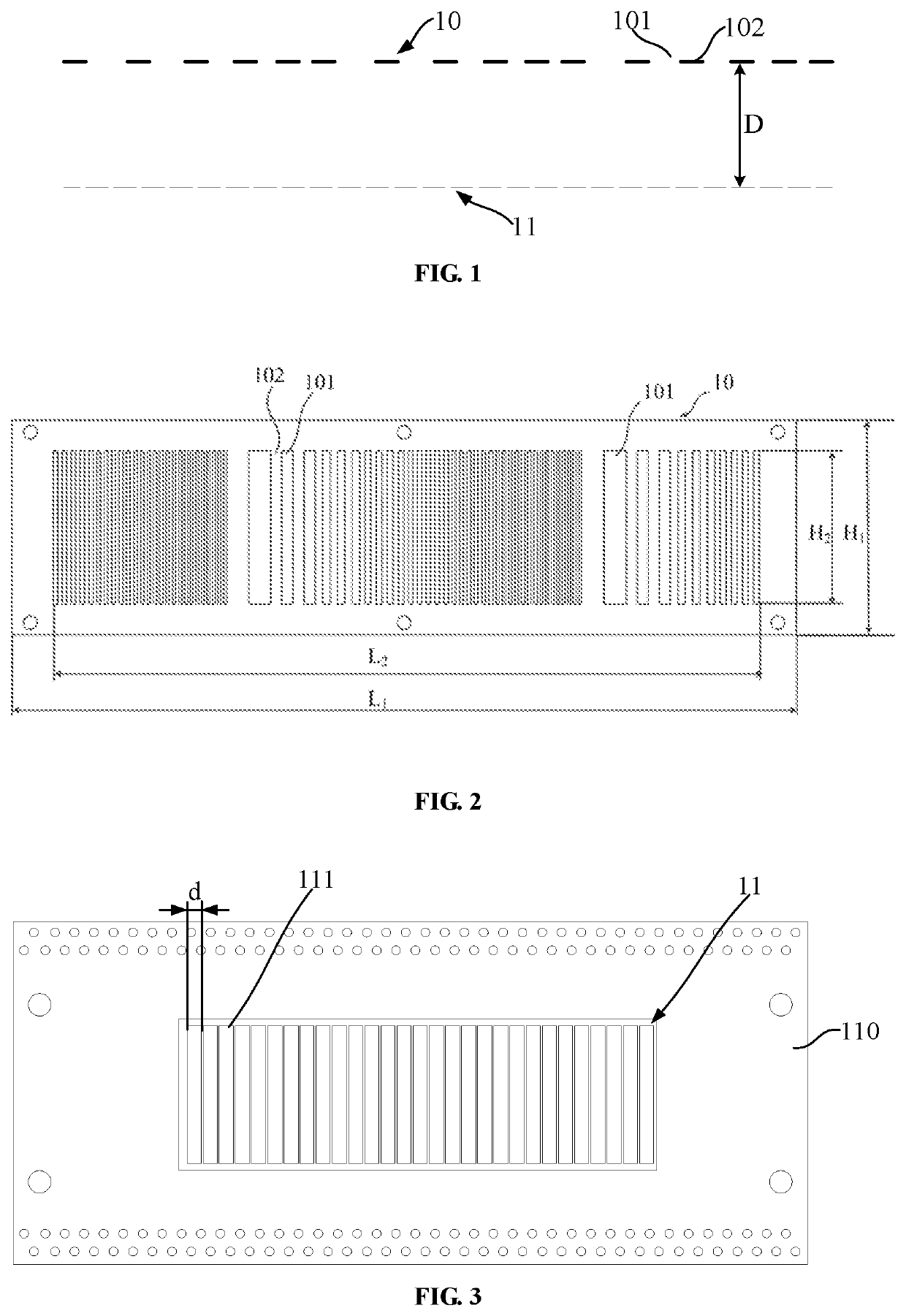
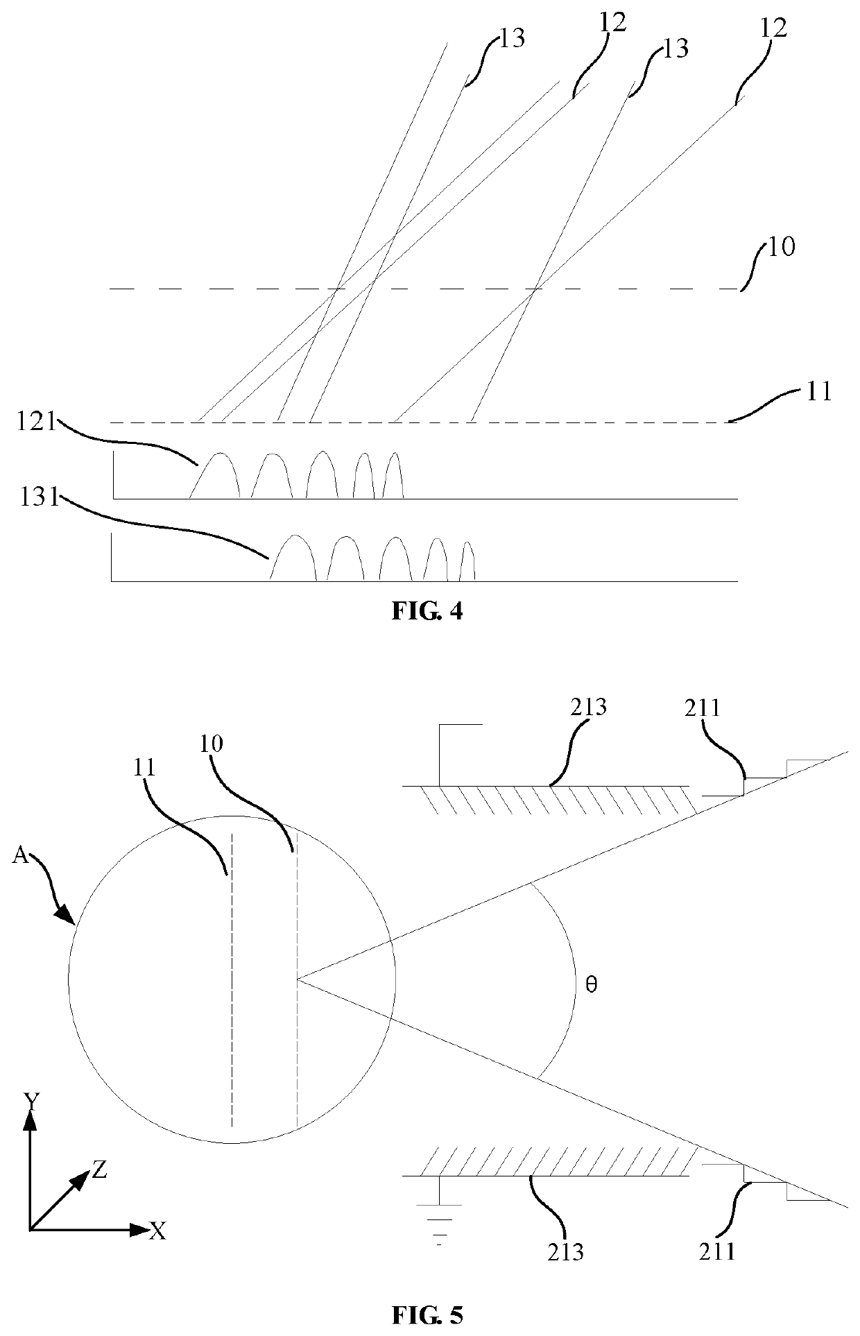
[0070]This embodiment provides a neutral atom imaging unit. In this embodiment, the neutral atom imaging unit includes at least one set of detection units as shown in FIG. 1. The detection unit includes a semiconductor detector line array 11 and at least one modulation unit grid 10. The modulation grid 10 is arranged in front of the semiconductor detector line array 11 and has a distance D from the semiconductor detector line array 11. The at least one modulation grid 10 and the at least one semiconductor detector line array are arranged in one-to-one correspondence. In the neutral atom imaging unit, the above-mentioned modulation grid 10 performs Fourier transform on the incident neutral atom;

[0071]FIG. 2 is a schematic structural diagram depicting a modulation grid 10 of the neutral atom imaging unit as shown in FIG. 1. In this embodiment, the modulation grid 10 includes a single-layer modulating multi-slit grid. As shown in FIG. 2, the modulation grid 10 includes a slit 101 and a...

embodiment 2

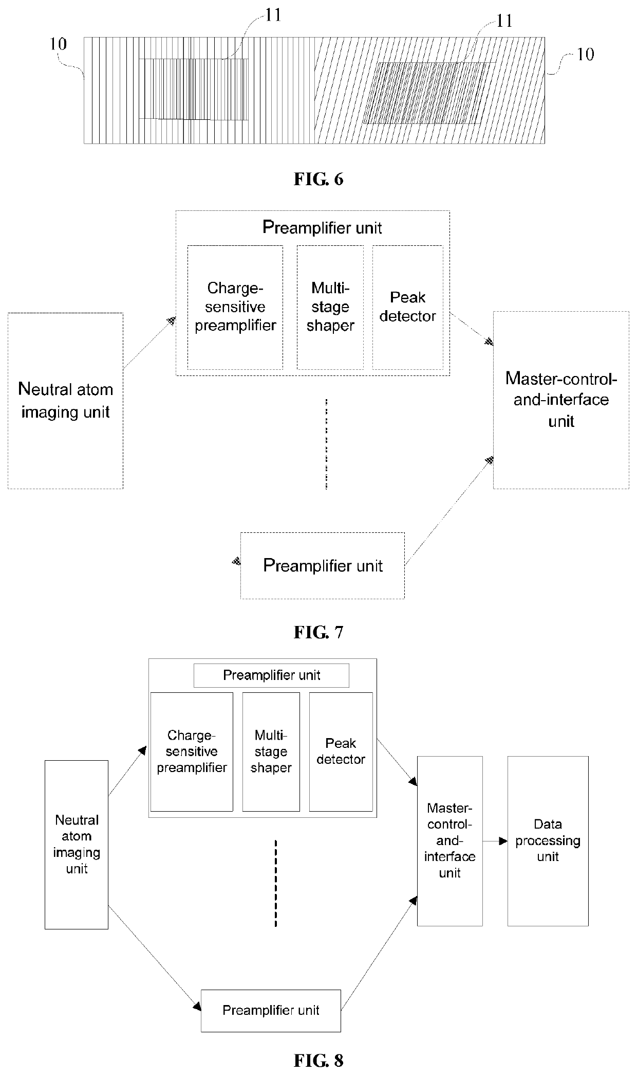
[0082]As shown in FIG. 7, this embodiment provides a neutral atom imager, which includes at least one neutral atom imaging unit, at least one preamplifier unit, and at least one master-control-and-interface unit; the at least one neutral atom imaging unit, the at least one preamplifier unit, and the at least one master-control-and-interface unit are electrically connected to each other.

[0083]The at least one neutral atom imaging unit detects and images neutral atoms. The at least one preamplifier unit reads the imaging data of the at least one neutral atom imaging unit, and preliminarily amplifies the imaging data.

[0084]The preamplifier unit includes a plurality of application-specific integrated circuits. The application-specific integrated circuits read the imaging signal of the at least one neutral atom imaging unit in real time and amplify the imaging signal.

[0085]Still referring to FIG. 7, in a preferred embodiment, the preamplifier unit includes at least one charge-sensitive p...

embodiment 3

[0089]This embodiment also provides a neutral atom imager. As shown in FIG. 9, the imaging probe 20 of the neutral atom imager further includes at least one housing 21. The housing 21 includes a base portion 212 and a fan-shaped portion 211 located above and fixedly connected to the base portion 212. In a more preferred embodiment, the fan-shaped portion 211 and the base portion 212 may be integrally formed, or may be fixedly connected by screw fastening, riveting, welding or the like. As shown in FIG. 9, the collimation-and-deflection module of the neutral atom imaging unit is provided on the fan-shaped portion 211. The outer panel of the fan-shaped portion 211 constitutes the collimator 214 of the collimation-and-deflection module. The deflection plate 213 is provided on the inner side of the fan-shaped panel of the outer panel. At least one detection unit of the neutral atom imaging unit is provided above the base portion 212 of the housing 21. The modulation grid 10 of the detec...


PUM


Abstract

The present disclosure provides a neutral atom imaging unit, a neutral atom imager, a neutral atom imaging method, and a space detection system. The neutral atom imaging unit includes at least one set of detection units, the at least one set of detection units includes: at least one semiconductor detector line array, each semiconductor detector line array includes a semiconductor detector strip composed of a plurality of semiconductor detectors; and at least one modulation grid. The modulation grid includes a slit and a slat forming the slit; the modulation grid includes a plurality of grid periods, each of the grid periods includes n slits, the width of the semiconductor detector strip is d, and the width (wi) of the i-th slit of the modulation grid satisfies the following relationship:
wi=ni×d.

Description

CROSS REFERENCE TO RELATED APPLICATION[0001]This application claims the benefits of priority to Chinese Patent Application No. CN 2020110184647, entitled “Neutral Atom Imaging Unit, Neutral Atom Imager, Neutral Atom Imaging Method, and Space Detection System”, filed with CNIPA on Sep. 24, 2020, the contents of which are incorporated herein by reference in its entirety.BACKGROUNDField of Disclosure[0002]The present disclosure relates to the field of neutral atom imaging, in particular, to a neutral atom imaging unit, a neutral atom imager, a neutral atom imaging method, and a space detection system.Description of Related Arts[0003]Holistic observation and global imaging have become one of the most promising approaches to solving geospatial physics issues. Energetic Neutral Atoms (ENA) are generated during the charge exchange process between ring current ions and geocorona hot particles. ENA is not bounded by magnetic fields and can leave the source area along a straight line at the s...

Claims


Application Information

Patent Timeline
IPC IPC(8): G01T1/24G01T3/08G01T1/36
CPCG01T1/24G21K1/025G01T1/36G01T3/08G01T1/2928
Inventor ZONG, QIUGANGWANG, YONGFUWANG, LINGHUAZOU, HONGCHEN, HONGFEIYU, XIANGQIANSHI, WEIHONGZHOU, LYU
Owner PEKING UNIV
Why Eureka
Try Eureka