Semiconductor device and method of manufacturing semiconductor device

Pending Publication Date: 2022-05-05
MITSUBISHI ELECTRIC CORP
View PDF0 Cites 0 Cited by
  • Summary
  • Abstract
  • Description
  • Claims
  • Application Information

AI Technical Summary

Benefits of technology

The patent aims to solve issues in semiconductor devices having a vertical structure, such as unstable breakdown voltage, reduced off-loss, improved control over turn-off operation, and better cutOff capability during turn-off. The problem is caused by crystal defects in the wafer during the formation of an N-type buffer layer. The patent achieves stable breakdown voltage characteristics, reduced off-loss, improved control over turn-off operation, and improved cut-off capability during turn-off while solving the issue caused by crystal defects.

Problems solved by technology

An impurity profile such as that described above observed in the buffer layer in the semiconductor device having the vertical structure encounters various problems in terms of bad controllability over turn-off operation and reduction in cutoff capability during turn-off.
While Japanese Patent Application Laid-Open No. 2020-027921 has mentions of the depth of the N-type buffer layer, and an impurity concentration and an impurity profile in the N-type buffer layer, it does not have mention of a relationship between crystal defect introduced into an Si wafer during formation of the N-type buffer layer and device characteristics, leading to poor feasibility of a power semiconductor element.
As will be described later, crystal defect introduced into the Si wafer is a significant factor to exert influence on controllability over a carrier plasma layer and electric field intensity that are important issues during dynamic operation of a power semiconductor element.

Method used


Image

  • Semiconductor device and method of manufacturing semiconductor device
  • Semiconductor device and method of manufacturing semiconductor device
  • Semiconductor device and method of manufacturing semiconductor device

Examples


first preferred embodiment

[0073]A semiconductor element provided in a power semiconductor device described in a first preferred embodiment is a relaxed field of cathode (RFC) diode having a structure in which a cathode layer is partially replaced with a P-type region.

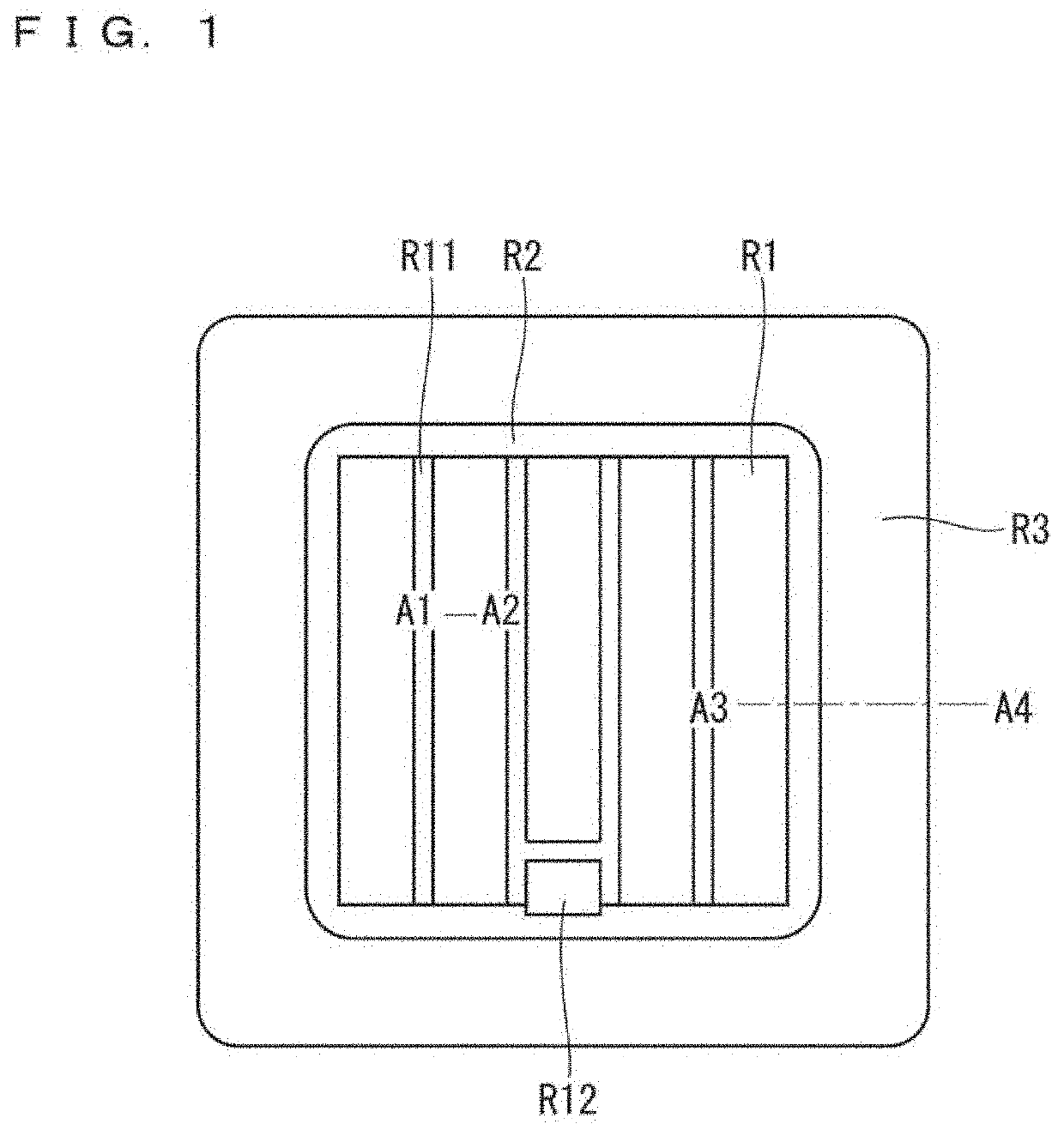
[0074]FIG. 1 is a plan view of a semiconductor device according to the first preferred embodiment. As shown in FIG. 1, the semiconductor device includes a plurality of active cell regions R1 provided at a central area of the device, a surface gate wiring part R11 provided between two of the active cell regions R1 adjacent to each other, and a gate pad part R12 provided in a partial region of the central area. An intermediate region R2 is provided in such a manner as to surround the active cell regions R1, the gate pad part R12, and the surface gate wiring part R11. An edge termination region R3 is provided in such a manner as to surround the intermediate region R2. The gate pad part R12 and the surface gate wiring part R11 may be absent in a dio...

second preferred embodiment

[0166]In a second preferred embodiment, the new structure N buffer layer 15 is applied to a PiN diode and it is verified that the new structure N buffer layer 15 applied in this way behaves in the same manner as in the first preferred embodiment.

[0167]FIG. 40 is a sectional view of a PiN diode showing a semiconductor element according to the second preferred embodiment and corresponding to a section taken along the line A1-A2 of FIG. 1. FIG. 41 is a sectional view showing an example of the structure of an outer peripheral part of a semiconductor device including the PiN diode according to the second preferred embodiment and corresponding to the section taken along the line A3-A4 of FIG. 1. The structures in FIGS. 40 and 41 include the N+ cathode layer 17 as the only cathode layer as a result of deletion of the P cathode layer 18 from the structures in FIGS. 2 and 3 described in the first preferred embodiment.

[0168]As shown in FIG. 41, a structure composed of a stack of the N− drift ...

third preferred embodiment

[0178]In a third preferred embodiment, the new structure N buffer layer 15 is applied to an IGBT and it is verified that the new structure N buffer layer 15 applied in this way behaves in the same manner as in the first preferred embodiment.

[0179]FIG. 45 is a sectional view showing a trench gate IGBT as a semiconductor element according to the third preferred embodiment and corresponding to a section taken along the line A1-A2 of FIG. 1. FIG. 46 is a sectional view showing an example of the structure of an outer peripheral part of a semiconductor device including the IGBT according to the third preferred embodiment and corresponding to the section taken along the line A3-A4 of FIG. 1.

[0180]The structure of the IGBT formed in the active cell region R1 will be described first by referring to FIG. 45. The semiconductor substrate forming the IGBT includes an N− drift layer 14 of an N type (first conductivity type). The semiconductor substrate includes an N-type N buffer layer 15 higher ...


PUM


Abstract

A semiconductor device includes: an N− drift layer of a first conductivity type formed in the semiconductor substrate; a P base layer formed on the N− drift layer; and an N buffer layer of the first conductivity type formed under the N− drift layer and higher in peak impurity concentration than the N− drift layer. The N buffer layer includes: a first buffer layer in which a trap level derived from lattice defect is not detected by a photoluminescence method; and a second buffer layer provided between the first buffer layer and the N− drift layer and in which two types of trap levels derived from lattice defect are detected by the photoluminescence method.

Description

BACKGROUND OF THE INVENTIONField of the Invention[0001]The present disclosure relates to a semiconductor device and a method of manufacturing a semiconductor device.Description of the Background Art[0002]A conventional vertical semiconductor device such as a trench gate insulated gate bipolar transistor (IGBT) or a P-intrinsic-N (PiN) diode has a vertical structure. In the IGBT, a region including an N-type drift layer, an N-type buffer layer, and a P-type collector layer is a region of the vertical structure. In the diode, a region including an N-type drift layer, an N-type buffer layer, and an N-type cathode layer is a region of the vertical structure. International Publication No. 2014 / 054121 discloses an IGBT with the vertical structure. Japanese Patent Application Laid-Open No. 2020-027921 discloses a configuration in which an N-type buffer layer has a stacked structure with a plurality of layers.[0003]In the conventional semiconductor device with the IGBT or the diode having t...

Claims


Application Information

Patent Timeline
IPC IPC(8): H01L29/739H01L29/868H01L29/06H01L29/66
CPCH01L29/7397H01L29/66333H01L29/0696H01L29/868H01L29/8613H01L29/7398H01L29/66136H01L29/66348H01L29/0684H01L29/0603H01L29/8611H01L29/0619H01L29/0638H01L23/3171H01L29/32H01L29/66128H01L29/404H01L29/407H01L29/0834H01L23/3192H01L2224/02166
Inventor NAKAMURA, KATSUMI
Owner MITSUBISHI ELECTRIC CORP
Why Eureka
Try Eureka