
High voltage edge termination structure for power semicondcutor devices and manufacturing method thereof

a technology of edge termination structure and power semiconductor, applied in the direction of semiconductor devices, basic electric elements, electrical apparatus, etc., can solve the problems of low applied voltage breakdown of devices, markedly sensitive jte structures to surface charge variations, and low voltage. , to achieve the effect of increasing the tolerance to surface charge, reducing the area of the structure, and high voltag

Pending Publication Date: 2022-05-19
YILMAZ HAMZA +1
View PDF21 Cites 2 Cited by
  • Summary
  • Abstract
  • Description
  • Claims
  • Application Information

AI Technical Summary

Benefits of technology

The present invention provides a way to increase the tolerance of high voltage edge termination structures while keeping their area minimal. This means that new HV termination structures can be implemented with greater flexibility.

Problems solved by technology

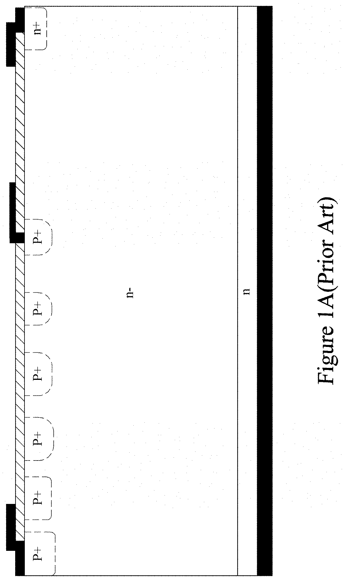
For instance, if the surface charge is high, the depletion width in the termination region shrinks, which may result in an increase of the electric field to critical values thereby causing the breakdown of the device at lower applied voltage.
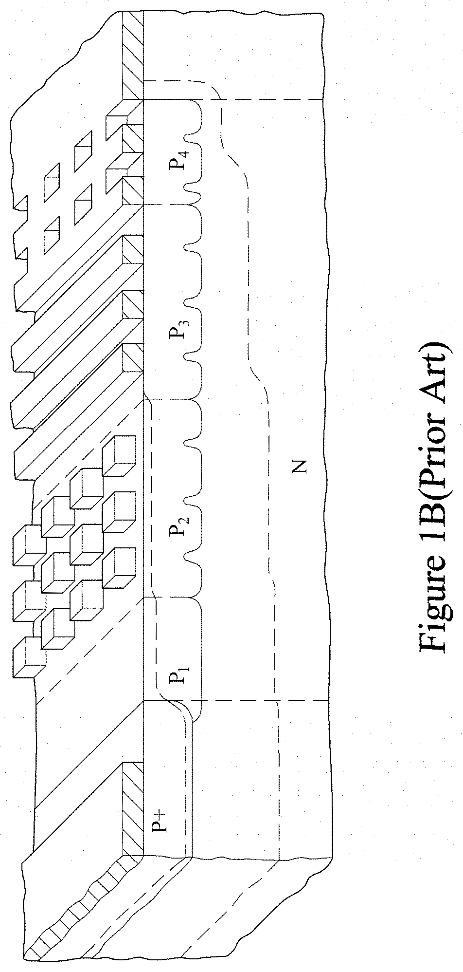
However, JTE structures are markedly sensitive to surface charge variations.

Method used


Image

  • High voltage edge termination structure for power semicondcutor devices and manufacturing method thereof
  • High voltage edge termination structure for power semicondcutor devices and manufacturing method thereof
  • High voltage edge termination structure for power semicondcutor devices and manufacturing method thereof

Examples


first embodiment

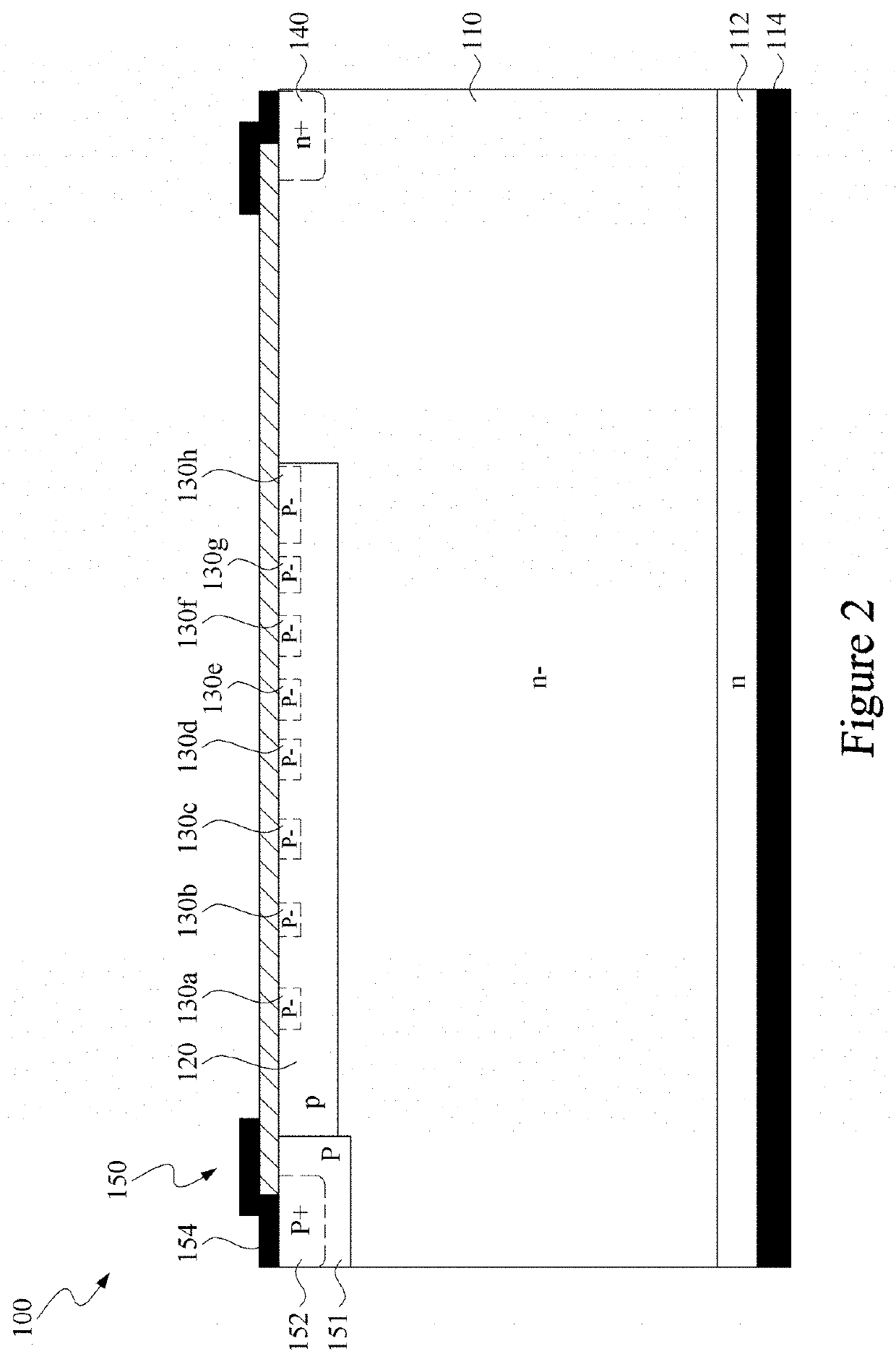
[0052]Please referring to FIG. 2, a high voltage edge termination structure featuring a laterally modulated JTE structure provided in accordance with the present invention will be discussed.

[0053]As illustrated in FIG. 2, the high voltage edge termination structure 100 comprises an N-type semiconductor body 110, a P-type JTE region 120, a plurality of P-type lightly doped regions 130a-130h, and an N-type heavily doped channel stop region 140.

[0054]There is an N-type semiconductor layer 112 with a doping concentration higher than that of the N-type semiconductor body 110 formed on a lower surface of the N-type semiconductor body 110. The N-type semiconductor layer 112 is utilized for reducing contact resistance between the N-type semiconductor body 110 and a cathode electrode 114 of the power semiconductor device.

[0055]The P-type JTE region 120 is formed in the top portion of the N-type semiconductor body 110. The P-type JTE region 120 is adjacent to the active region 150 of the powe...

second embodiment

[0066]Referring to FIG. 3, a high voltage edge termination structure featuring a JTE structure with field plates provided in accordance with the present invention will be discussed.

[0067]As illustrated in FIG. 3, the high voltage edge termination structure 200 comprises an N-type semiconductor body 210, a P-type JTE region 220, an N-type heavily doped channel stop region 240, and a plurality of field plates 260 (three field plates are shown).

[0068]There is an N-type semiconductor layer 212 with a doping concentration higher than that of the N-type semiconductor body 210 formed on a lower surface of the N-type semiconductor body 210. The N-type semiconductor layer 212 is utilized for reducing contact resistance between the N-type semiconductor body 210 and a cathode electrode 214 of the power semiconductor device.

[0069]The P-type JTE region 220 is formed in the top portion of the N-type semiconductor body 210, i.e. the portion close to the upper surface thereof. The P-type JTE region...

third embodiment

[0073]Referring to FIG. 4, a high voltage edge termination structure featuring a JTE structure with depletable guard rings and field plates provided in accordance with the present invention will be discussed.

[0074]As illustrated in FIG. 4, the high voltage edge termination structure 300 comprises an N-type semiconductor body 310, a P-type JTE region 320, an N-type heavily doped channel stop region 340, a plurality of field plates 360 (three field plates are shown), and a plurality of P-type depletable guard rings 370 (four depletable guard rings are shown).

[0075]There is an N-type semiconductor layer 312 with a doping concentration higher than that of the N-type semiconductor body 310 formed on a lower surface of the N-type semiconductor body 310. The N-type semiconductor layer 312 is utilized for reducing contact resistance between the N-type semiconductor body 310 and a cathode electrode 314 of the power semiconductor device.

[0076]The P-type JTE region 320 is formed in top portion...


PUM

PropertyMeasurementUnit
voltagesaaaaaaaaaa
surface potentialaaaaaaaaaa

Abstract

A high voltage edge termination structure for a power semiconductor device is provided. The high voltage edge termination structure comprises a semiconductor body of a first conductive type, a JTE region of a second conductive type, a heavily doped channel stop region of the first conductive type, and a plurality of field plates. The JTE region is formed in the semiconductor body, wherein the JTE region is adjacent to an active region of the power semiconductor device. The heavily doped channel stop region is formed in the semiconductor body, wherein the heavily doped channel stop region is spaced apart from the JTE region. The plurality of field plates is formed on the JTE region.

Description

BACKGROUNDField of the Invention[0001]The present invention relates to semiconductor devices, and more particularly to high voltage edge termination structures for power semiconductor devices and manufacturing method thereof.Description of the Related Art[0002]Reliable power semiconductor devices require high voltage edge termination structures. The high voltage edge termination structures nowadays are presented in various forms, including field plate, floating guard ring, junction termination extension (JTE), as well as combinations of floating guard ring with field plate structures. Additionally, there are combinations of these basic termination techniques applied to the latest wide bandgap semiconductors, such as the variably laterally doped zone with decreasing concentration termination disclosed in U.S. Pat. No. 8,564,088B2, the double guard ring edge termination for SiC disclosed in U.S. Pat. No. 9,640,609B2.[0003]The selection of high voltage edge termination structures is de...

Claims


Application Information

Patent Timeline
Patent Type & Authority Applications(United States)
IPC IPC(8): H01L29/40H01L29/06H01L21/265
CPCH01L29/404H01L21/265H01L29/0638H01L29/0615H01L29/8611H01L29/0619H01L29/66128
Inventor YILMAZ, HAMZAMRINAL, ARYADEEP
Owner YILMAZ HAMZA
Learn More