
Semiconductor device

Pending Publication Date: 2022-05-26
ROHM CO LTD
View PDF0 Cites 0 Cited by
  • Summary
  • Abstract
  • Description
  • Claims
  • Application Information

AI Technical Summary

Benefits of technology

The present invention aims to provide a solution to prevent the size of a circuit board on which a semiconductor device is mounted from increasing while reducing the surge voltage generated in the device.

Problems solved by technology

Generally, driving the switching elements causes generation of a surge voltage in the semiconductor device.
An excessively large surge voltage may destroy the switching elements.
This leads to an increase in size of the circuit board, which leaves room for improvement.

Method used


Image

  • Semiconductor device
  • Semiconductor device
  • Semiconductor device

Examples


first embodiment

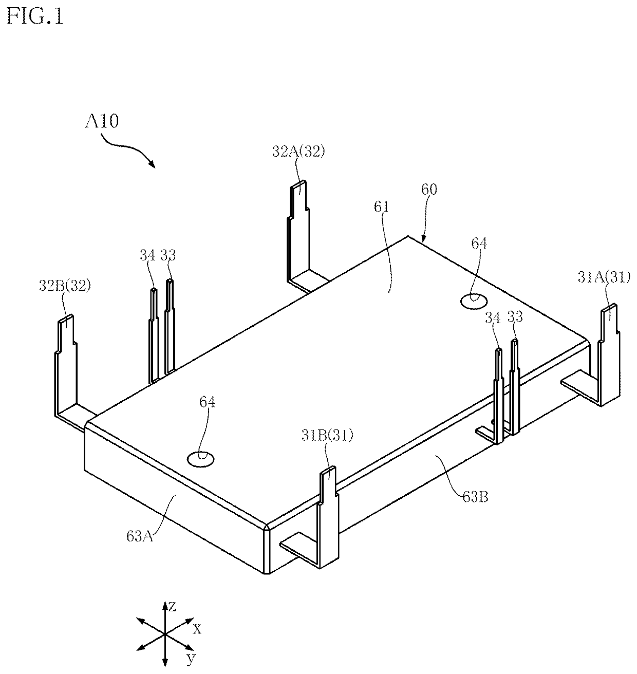
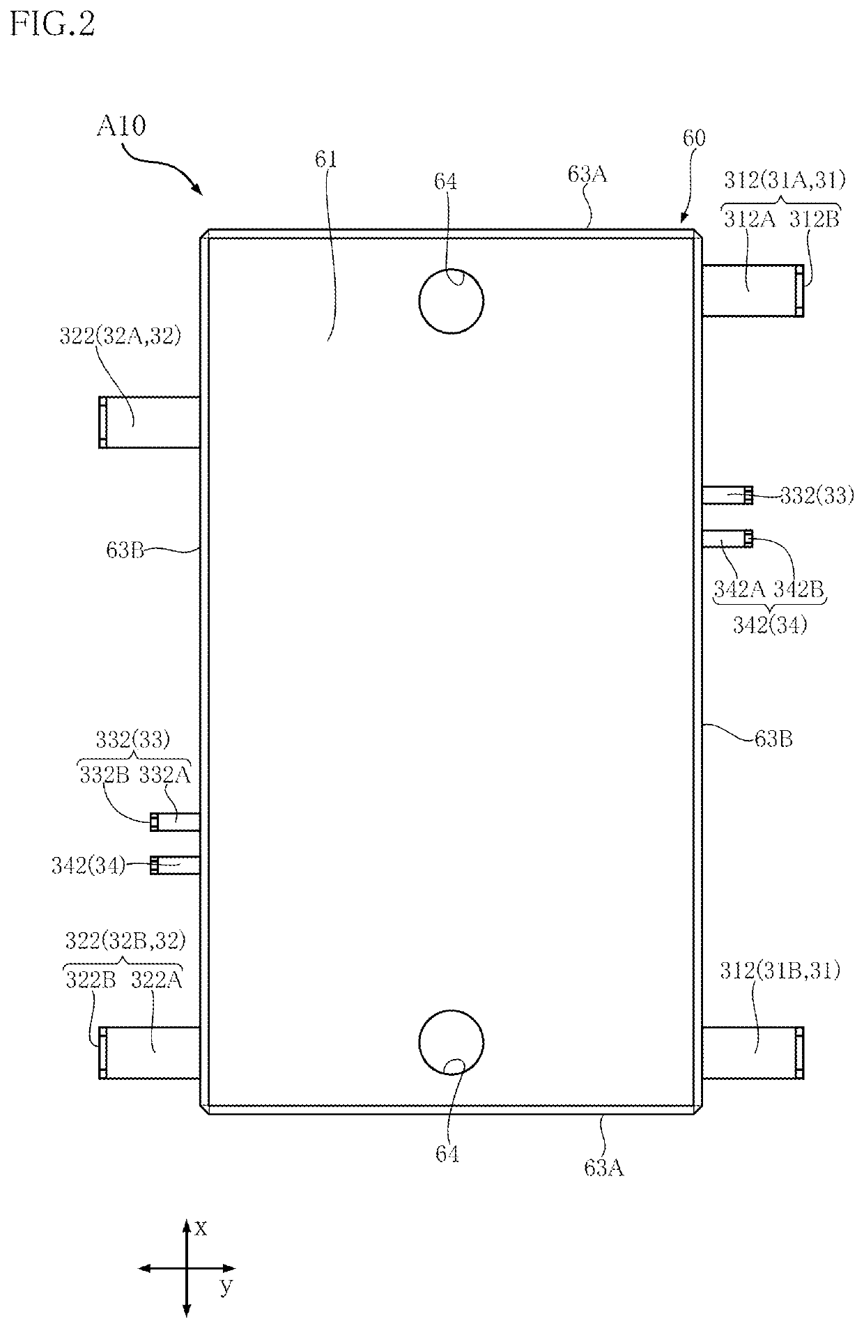
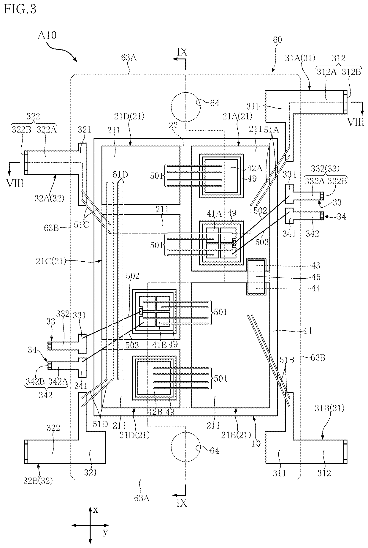
[0052]A semiconductor device A10 is described below with reference to FIGS. 1-15. The semiconductor device A10 includes a support member 10, a first switching element 41A, a second switching element 41B, a first diode 42A, a second diode 42B, a first passive element 43, a second passive element 44, an electrical conductor 45 and a sealing resin 60 (see FIGS. 3, 8, 9 and 11-13, for example). In addition to these, as shown in FIG. 3 (and FIG. 1), the semiconductor device A10 includes a pair of input terminals 31, a pair of output terminals 32, a pair of gate terminals 33, a pair of detection terminals 34, a plurality of first conduction members 51A, a plurality of second conduction members 51B, a plurality of third conduction members 51C, and a plurality of fourth conduction members 51D. In the semiconductor device A10, DC power is converted into AC power by driving the first switching element 41A and the second switching element 41B. The semiconductor device A10 is used for a drivin...

second embodiment

[0101]A semiconductor device A20 will be described with reference to FIGS. 16 and 17. In these figures, the elements that are identical or similar to those of the semiconductor device A10 are denoted by the same reference signs, and the description is omitted. In FIG. 16, the sealing resin 60 is illustrated as transparent.

[0102]The semiconductor device A20 differs from the semiconductor device A10 in that it includes an electrical insulator 46.

[0103]As shown in FIGS. 16 and 17, the electrical insulator 46 is located between the first passive element 43 and the second passive element 44. The electrical insulator 46 is thermally conductive. The electrical insulator 46 has an insulating body 461 and an adhesive layer 462. The insulating body 461 is a ceramic material containing silicon nitride or aluminum nitride, for example. Thus, the insulating body 461 has a relatively high thermal conductivity. The upper surface of the insulating body 461 is in contact with the electrical conduct...

third embodiment

[0107]A semiconductor device A30 is described with reference to FIGS. 18 and 19. In these figures, the elements that are identical or similar to those of the semiconductor device A10 are denoted by the same reference signs, and the description is omitted. In FIG. 18, the sealing resin 60 is illustrated as transparent.

[0108]The semiconductor device A30 differs from the semiconductor device A10 in configuration of the first passive element 43, the second passive element 44 and the electrical conductor 45.

[0109]As shown in FIGS. 18 and 19, in the semiconductor device A30, the first electrode 431 and the second electrode 432 of the first passive element 43 are spaced apart from each other in the first direction x. The third electrode 441 and the fourth electrode 442 of the second passive element 44 are also spaced apart from each other in the first direction x. As viewed along the thickness direction z, the electrical conductor 45, the second electrode 432 and the third electrode 441 a...


PUM


Abstract

A semiconductor device includes a support member, a first switching element, a second switching element, a first passive element, a second passive element, and an electrical conductor. The support member includes a plurality of wiring parts, and the plurality of wiring parts include a first wiring section and a second wiring section spaced apart from each other in a first direction perpendicular to the thickness direction of the support member. The first switching element is electrically connected to the first wiring section. The second switching element is electrically connected to the first switching element and the second wiring section. The first passive element has a first electrode and a second electrode, and the first electrode is bonded to the first wiring section. The second passive element has a third electrode and a fourth electrode, and the fourth electrode is bonded to the second wiring section. The electrical conductor connects the second electrode and the third electrode to each other. At least one of the first passive element and the second passive element is a capacitor.

Description

TECHNICAL FIELD[0001]The present disclosure relates to a semiconductor device including a plurality of switching elements.BACKGROUND ART[0002]Conventionally, semiconductor devices with a plurality of switching elements (e.g. MOSFET, IGBT etc.) are widely known. Patent Document 1 discloses an example of such a semiconductor device. Generally, driving the switching elements causes generation of a surge voltage in the semiconductor device. The surge voltage tends to increase as a larger current flows through the switching elements or the switching elements are driven at a higher speed. An excessively large surge voltage may destroy the switching elements.[0003]The semiconductor device disclosed in the Patent Document 1 has a plurality of snubber terminals, which are connected to a plurality of snubber circuits for reducing the surge voltage. However, the snubber circuits are formed on a circuit board on which the semiconductor device is mounted. This leads to an increase in size of the...

Claims


Application Information

Patent Timeline
IPC IPC(8): H01L25/16H01L25/07H01L25/18H01L23/00H01L23/31H01L23/373
CPCH01L25/16H01L2924/13091H01L25/18H01L24/32H01L24/48H01L24/73H01L23/3107H01L23/3735H01L2224/32225H01L2224/48175H01L2224/48225H01L2224/73265H01L2924/1205H01L2924/1207H01L2924/10272H01L2924/12032H01L25/072H01L23/50H01L23/49531H01L23/49575H01L23/49562H01L23/49541H01L2224/49431H01L2224/49175H01L2924/181H01L2224/48091H01L2224/48247H01L2224/0603H01L2224/4903H01L2924/19107H01L2224/4917H01L2224/06181H01L23/62H01L2224/49111H01L2924/00012H01L2924/00014H01L2224/48227
Inventor KANDA, TAKUMI
Owner ROHM CO LTD
Features
  • Generate Ideas
  • Intellectual Property
  • Life Sciences
  • Materials
  • Tech Scout
  • Unparalleled Data Quality
  • Higher Quality Content
  • 60% Fewer Hallucinations
Learn More