Method for manufacturing a polysilicon soi substrate including a cavity

a manufacturing method and polysilicon soi technology, applied in the direction of coatings, microstructural devices, microstructured technology, etc., can solve the problems of high cost, complex method, and high cost of cavity soi wafer manufacturing process, and achieve cost-effective and robust products.

Pending Publication Date: 2022-06-02
ROBERT BOSCH GMBH
View PDF4 Cites 1 Cited by
  • Summary
  • Abstract
  • Description
  • Claims
  • Application Information

AI Technical Summary

Benefits of technology

[0010]It is an object of the present invention to provide an alternative manufacturing method for manufacturing a polysilicon SOI substrate including a cavity, which is cost effective and results in a robust product.

Problems solved by technology

The manufacturing process for cavity SOI wafers is complex.
A second wafer is bonded on the first wafer using a relatively costly and complex direct bonding method (FIG. 1B).
This manufacturing method has the disadvantage that this method is very complex.
Two costly and complex direct bonding steps are also necessary to be able to achieve a precisely defined layer thickness above the cavity.
Furthermore, cavity SOI wafers are very sensitive.
Edges arise at the wafer edge due to the direct bonding method, which may easily result in wafer breakage if they strike lightly against an obstacle in the manufacturing process.

Method used


Image

  • Method for manufacturing a polysilicon soi substrate including a cavity
  • Method for manufacturing a polysilicon soi substrate including a cavity
  • Method for manufacturing a polysilicon soi substrate including a cavity

Examples


Embodiment Construction

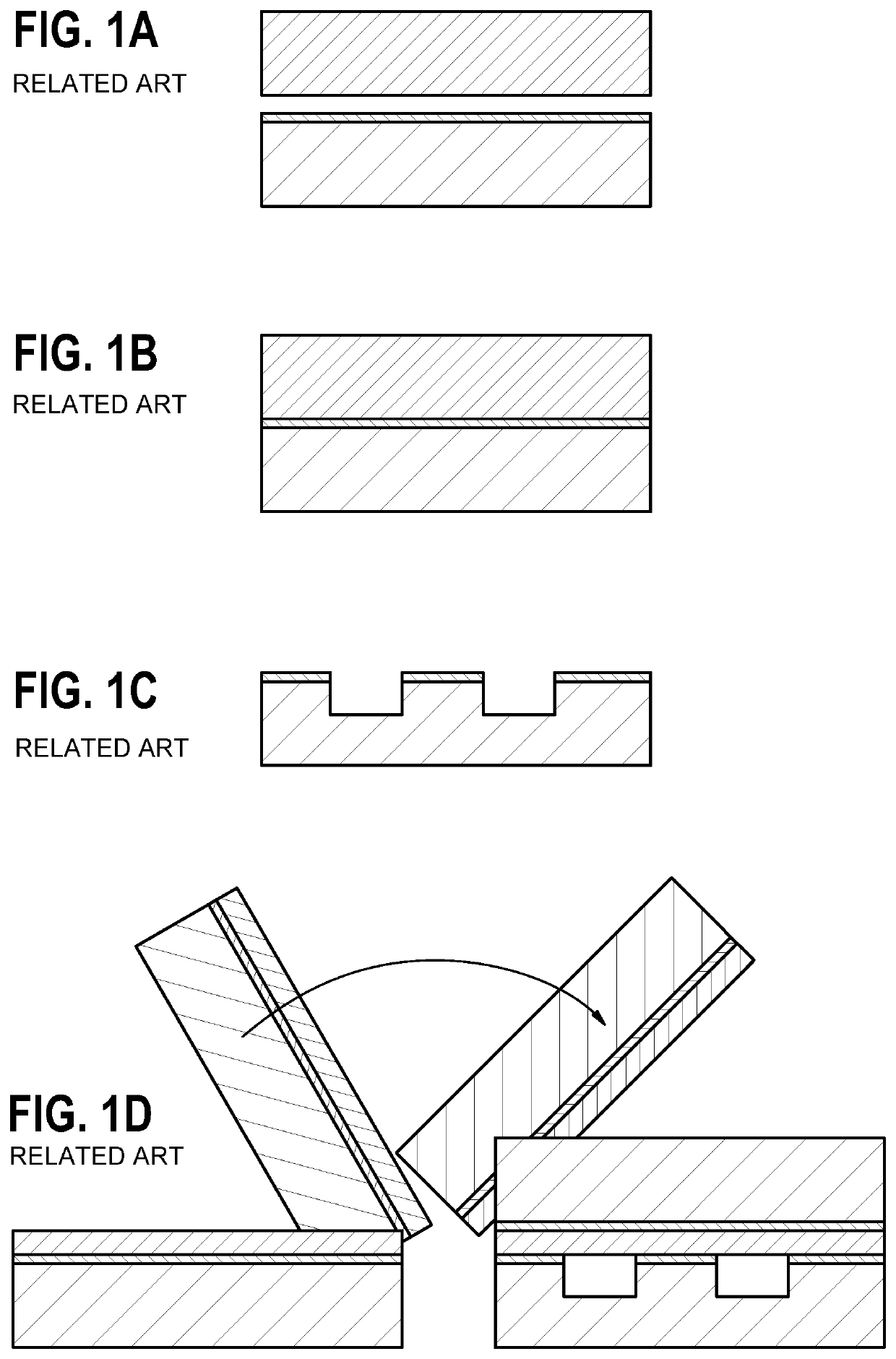
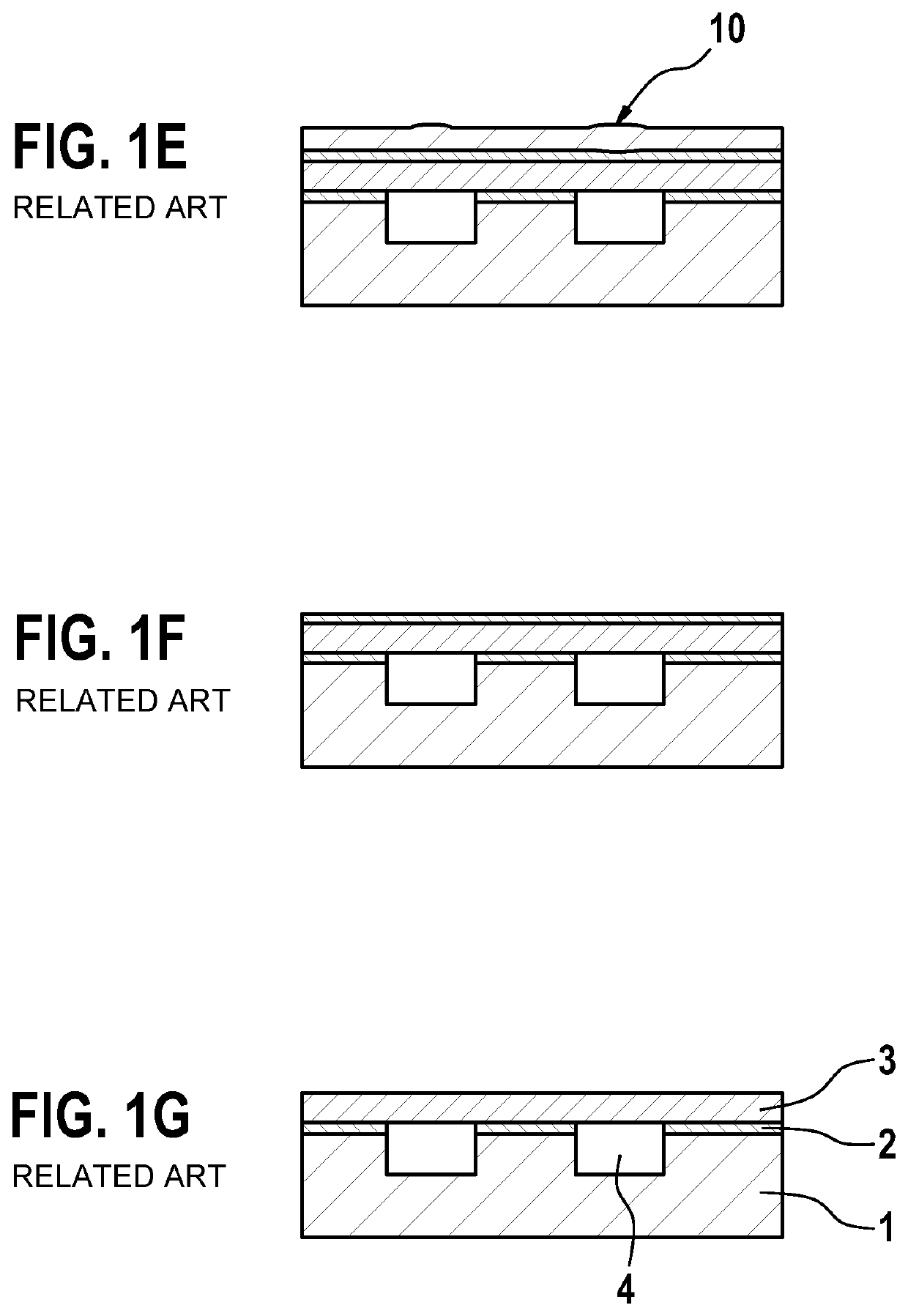
[0024]FIGS. 1A through 1G show a method for manufacturing an SOI substrate including a cavity in the related art.

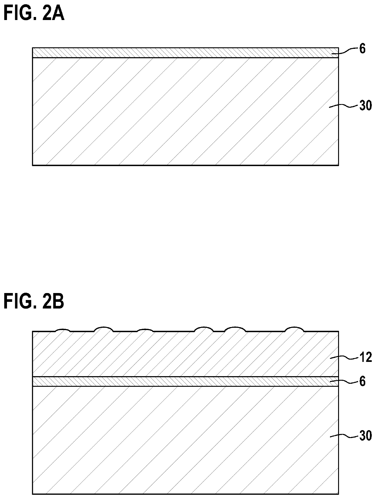
[0025]FIGS. 2A through 2J show a method according to the present invention for manufacturing an SOI substrate including a cavity in successive processing steps of the substrate.

[0026]A first oxide layer 6 is deposited or grown on a substrate 30, preferably on a monocrystalline silicon wafer (FIG. 2A). This first layer does not necessarily have to be an oxide layer according to the present invention, another dielectric layer such as a nitride or an oxynitride layer may also be used. An oxide layer is preferably grown via an oxidation process on the silicon wafer. Layers manufactured in this way have a very homogeneous oxide thickness and a very high quality.

[0027]In the next step, a first polysilicon layer 12 is deposited. This may be an LPCVD deposition or a thin LPCVD deposition including a subsequent fast epitaxial poly-deposition (FIG. 2B).

[0028]In an optional step, wh...


PUM

PropertyMeasurementUnit
thicknessaaaaaaaaaa
thicknessaaaaaaaaaa
thickaaaaaaaaaa

Abstract

A method for manufacturing a polysilicon SOI substrate including a cavity. The method includes: providing a silicon substrate including a sacrificial layer thereon; producing a first polysilicon layer on the sacrificial layer; depositing a structuring layer on the first polysilicon layer; introducing trenches through the structuring layer, the first polysilicon layer, and the sacrificial layer up to the silicon substrate; producing a cavity in the silicon substrate by etching, an etching medium being conducted thereto through the trenches; producing a second polysilicon layer on the first polysilicon layer, the trenches being thereby closed. A micromechanical device is also described.

Description

BACKGROUND INFORMATION[0001]Cavity SOI substrates (for example, substrates from Okmetic) are available, which are used as the basis for many MEMS components (FIG. 1G).[0002]SOI substrates (SOI: silicon on insulator) include a thin monocrystalline silicon layer 3 on a substrate 1, usually on a silicon wafer, which has a very precisely defined thickness (typically 0.5-50 μm) and which is connected to the substrate via a dielectric layer 2, usually an oxide layer (typically 0.1-5 μm). Both properties, the defined thickness and the insulation layer, are very important for MEMS applications.[0003]In cavity SOI substrates, cavities 4 are additionally provided below the thin silicon layer. Freestanding structures may be generated very easily in the thin silicon layer via a trenching process in these areas. The well-defined layer thickness is important to be able to generate structures having well-defined mechanical properties.[0004]If cavity SOI substrates are used, sacrificial layer etchi...

Claims


Application Information

Patent Timeline
Patent Type & Authority Applications(United States)
IPC IPC(8): H01L21/762H01L21/02B81C1/00B81B3/00
CPCH01L21/7624H01L21/02595B81B3/0021B81C1/00182H01L21/02532B81C1/00047H01L21/764H01L21/76278
Inventor REINMUTH, JOCHENSCHMOLLNGRUBER, PETER
Owner ROBERT BOSCH GMBH
Why Eureka
Try Eureka