Quantum device and method for producing the same
- Summary
- Abstract
- Description
- Claims
- Application Information
AI Technical Summary
Benefits of technology
Problems solved by technology
Method used
Image
Examples
first embodiment
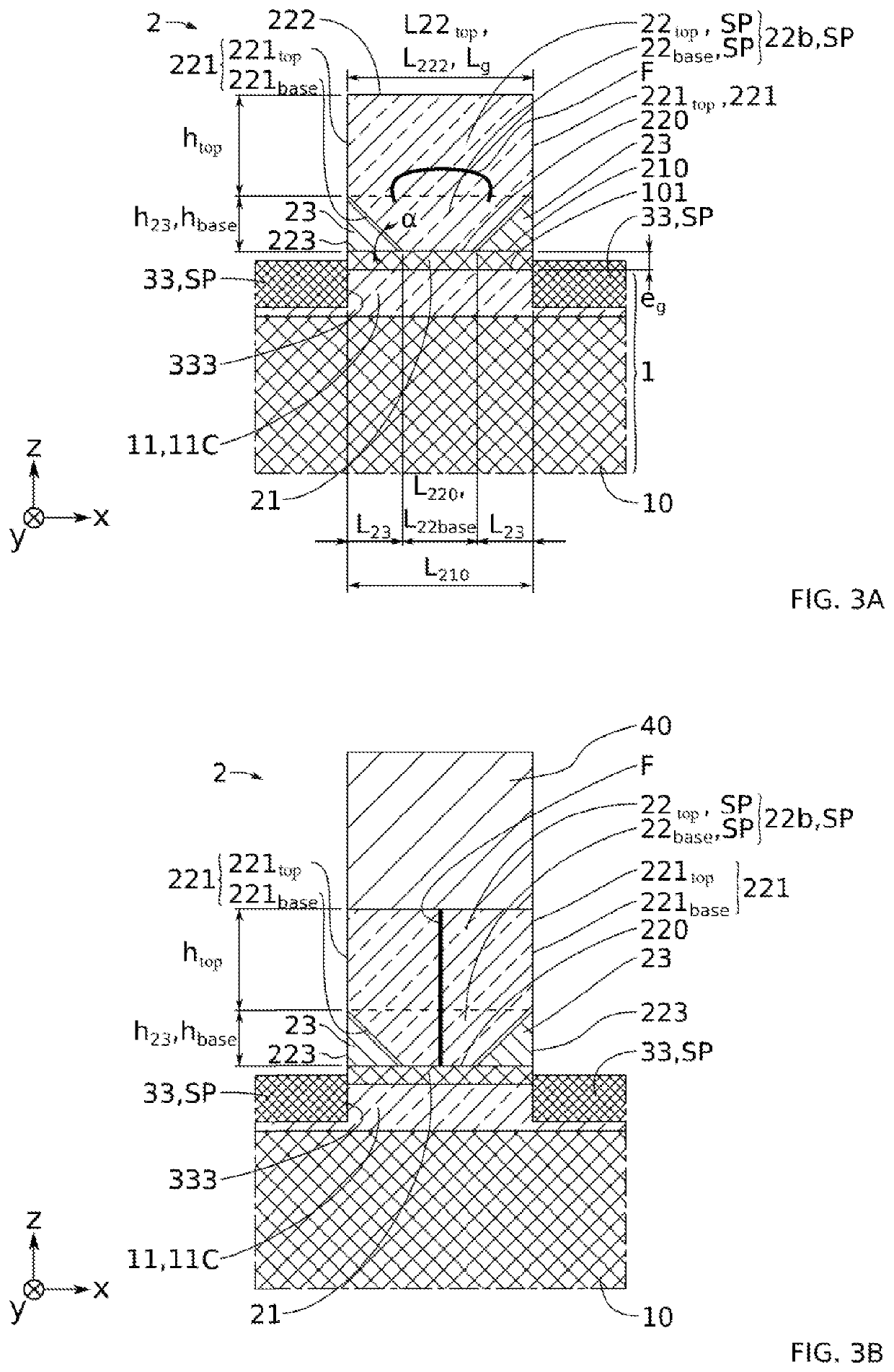
[0108]In the device shown in FIG. 3A, the silicidation front F can be in part substantially parallel to the top 222. This typically indicates that the superconducting region SP has been formed by diffusion from the top 222.
second embodiment
[0109]In the device shown in FIG. 3B, the transistor pattern 2 is overlaid by a hard mask 40 typically based on silicon nitride SiN or SiO2. In this embodiment, the silicidation front F can be substantially vertical. This typically indicates that the superconducting region SP has been formed by lateral diffusion from the sidewalls 221top.
[0110]FIG. 4 and FIG. 5A to 5I show embodiments of the method according to the invention. These embodiments of the method in particular allow the devices described hereinabove, according to the first and second embodiments, to be obtained.
[0111]As shown in FIG. 5A, a substrate 1 carrying a stack of a dielectric layer 21c and a gate layer 22c is previously provided 100. The dielectric layer 21c can be formed by oxidation or deposition on the front face 101 of the substrate 1, typically on the active layer 11 of an SOI-type substrate 1. The gate layer 22c can be formed by deposition on the top face 210c of the dielectric layer 21c. The gate layer 22c ...
PUM
 Abstract
Description
Claims
Application Information


