Optical transmitter
- Summary
- Abstract
- Description
- Claims
- Application Information
AI Technical Summary
Benefits of technology
Problems solved by technology
Method used
Image
Examples
first embodiment
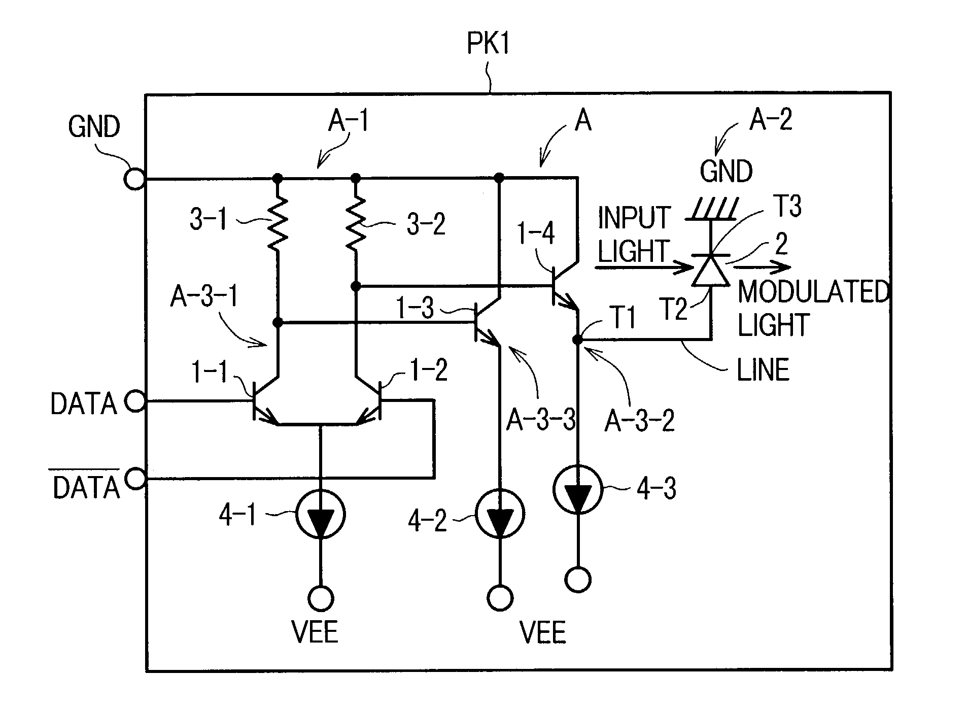
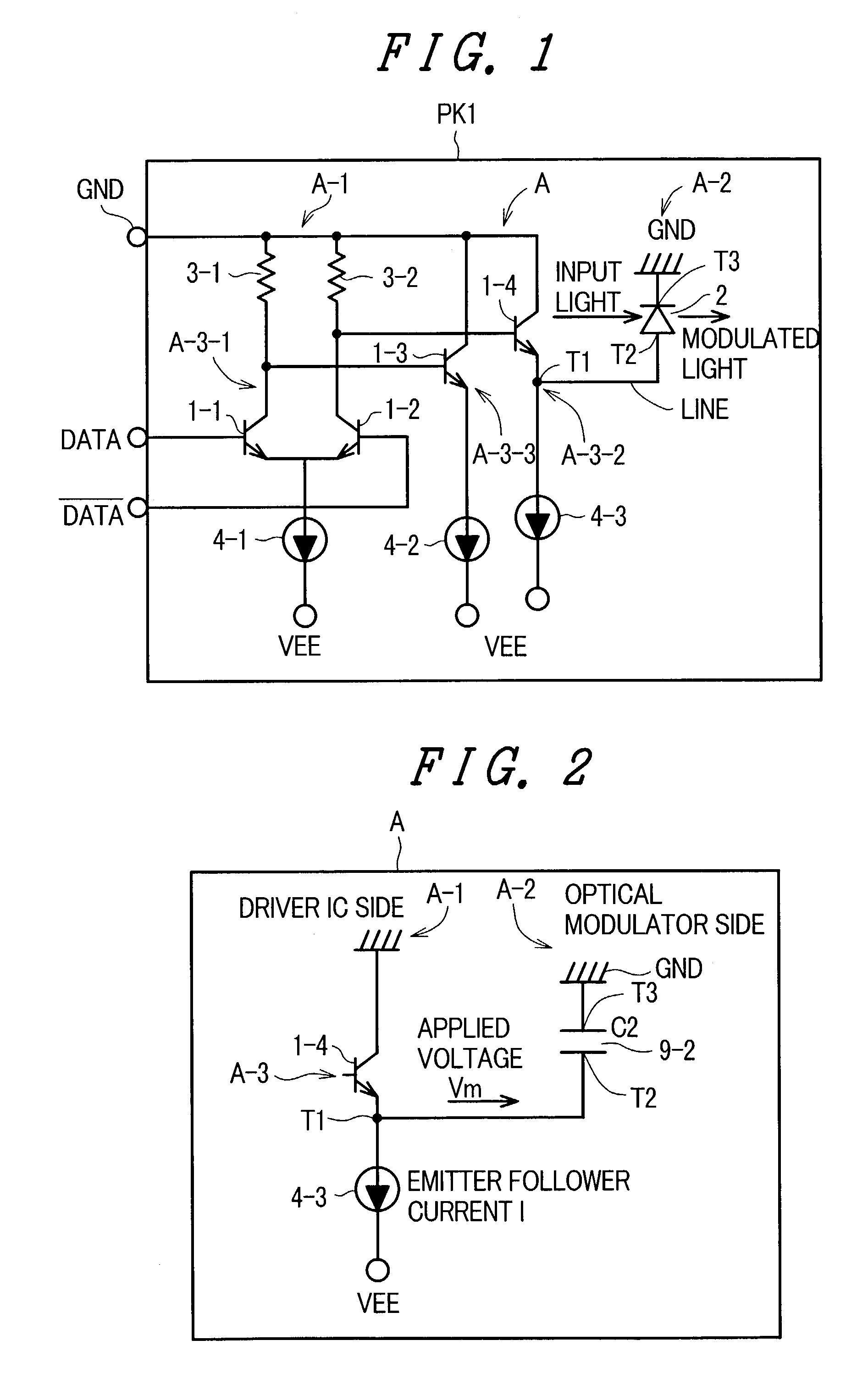
[0064]According to the present invention, the optical transmitter employs the emitter follower as an output circuit, and thereby output impedance can be lowered. That is, a driver system having a CR time constant limit is replaced with an impedance driver system having a low capacitance by providing the emitter follower circuit 1-4 at output stage of the driver circuit A-1.
[0065]The operating frequency is determined based on the charge-and-discharge time of the capacitance C of the optical modulator by current I flowing to an emitter follower, and thus the maximum operating frequency can be raised by adjusting the current I flowing to the emitter follower circuit 1-4. In this case, the driver circuit A-1 and the optical modulator A-2 are preferably arranged so as to have a distance therebetween, which can be regarded as a lumped constant even at the maximum operating frequency.
[0066]It is noted that the bipolar transistor is used as a transistor in FIG. 1, though, for example, a fie...
second embodiment
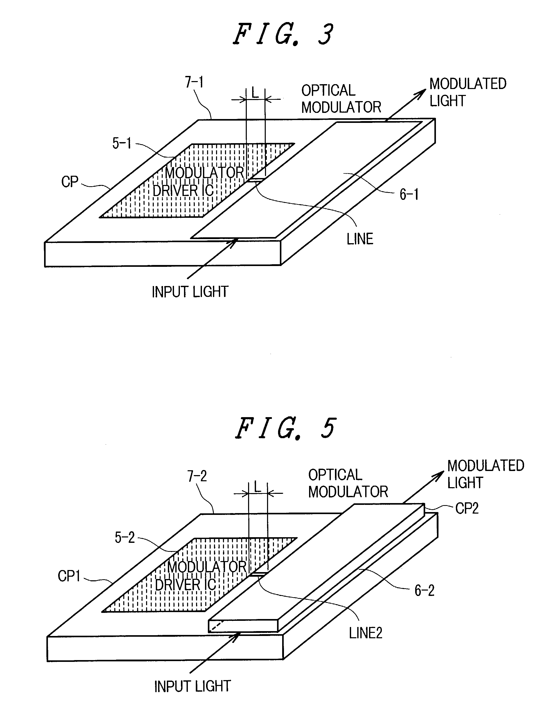
[0072]Next, an optical transmitter according to the present invention is described with reference to FIGS. 5, 6A and 6B, and if necessary, also to FIG. 1.
[0073]As shown in FIGS. 5 and 6A, the optical transmitter of the present embodiment has a first chip CP1 on which a driver circuit 5-2 is formed, and a second chip CP2 formed on the first chip CP1, the second chip CP2 having an EA type optical modulator 6-2 formed thereon. An output terminal at output stage of the driver circuit 5-2 is connected to an input terminal of the optical modulator 6-2 via a wiring LINE 2.
[0074]As shown in FIG. 6B, the optical transmitter B of the present embodiment, for example, is formed in an InP substrate 31. In the semi-insulating InP substrate 31, an n-type impurity diffusion layer 21a is formed. Adjacent to this n-type impurity diffusion layer 21a, mounted on the InP substrate 31 is an EA type optical modulator chip which has a lamination structure of a p-type InP substrate 31b and an n-type conduct...
third embodiment
[0080]Next, before describing an optical transmitter of the present invention, a second consideration by the present inventors is described with reference to FIG. 16.
[0081]The optical transmitter as shown in FIG. 16 has a high level adjustment circuit provided between an optical modulator and a driver circuit, in addition to the optical transmitter as shown in FIG. 14.
[0082]As shown in FIG. 16, the level adjustment circuit 141 is provided on the way of the way of a wiring LINE 100 between a driver circuit 100-1 and an optical modulator 100-2 (between an output terminal at the output circuit of driver circuit 100-1 and an input terminal of the optical modulator 100-2). High level adjustment can be performed by making more current flow towards the level adjustment circuit 141. However, when the level adjustment circuit 141 is provided, parasitic capacitance increase, thereby causing a drawback, that is lowering the maximum operating frequency fm.
[0083]Hence, the present inventors devi...
PUM
 Abstract
Description
Claims
Application Information


