Chip-on-board type photoelectric device

a photoelectric device and chip-on-board technology, applied in the field of photoelectric technologies, can solve the problems of poor stability, metal substrate and chip electrode corrosion, and poor stability

Pending Publication Date: 2022-08-11
KAISTAR LIGHTING (XIAMEN) CO LTD
View PDF0 Cites 0 Cited by
  • Summary
  • Abstract
  • Description
  • Claims
  • Application Information

AI Technical Summary

Problems solved by technology

However, due to KSF material has strong metal corrosiveness, it will corrode metal structures such as a metal substrate and chip electrodes of the COB type light source.
Moreover, it will also react with water and air, resulting

Method used


Image

  • Chip-on-board type photoelectric device
  • Chip-on-board type photoelectric device
  • Chip-on-board type photoelectric device

Examples


first embodiment

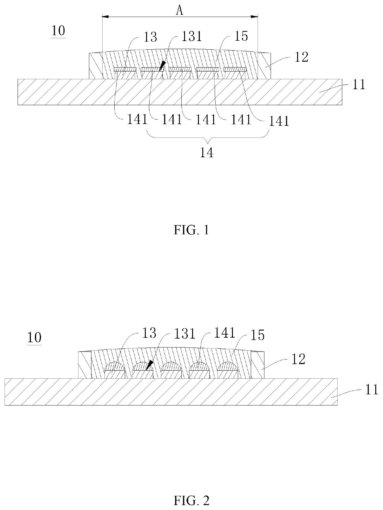
[0034]Referring to FIG. 1, the first embodiment of the disclosure provides a chip-on-board (COB) type photoelectric device. As shown in FIG. 1, the COB type photoelectric device 10 may include a metallic substrate 11, a dam 12 (also referred to as enclosure), multiple first photoelectric elements 13, a manganese-containing potassium fluorosilicate (hereinafter shorted as KSF) phosphor based layer 14, and an isolation layer 15.

[0035]The metallic substrate 11 may include a photoelectric element fixing area A. The dam 12 is disposed on the metallic substrate 11 and surrounding the photoelectric element fixing area A. The multiple first photoelectric elements 13 are disposed on the metallic substrate 11 and in the photoelectric element fixing area A. The KSF phosphor based layer 14 is disposed on the multiple first photoelectric elements 13 and being not in contact with (also referred to as spaced from) the metallic substrate 11. The KSF phosphor based layer 14 includes a KSF phosphor, ...

second embodiment

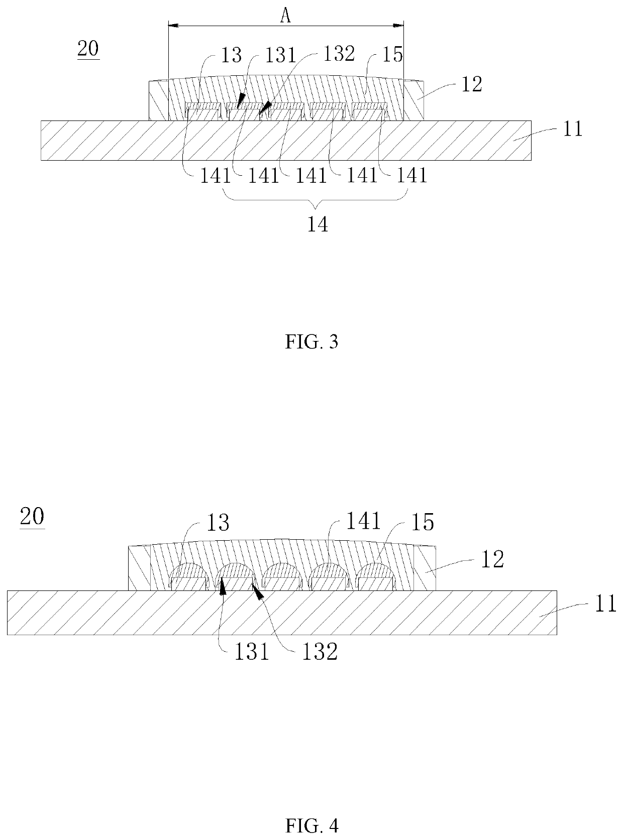
[0046]Referring to FIG. 3, the second embodiment of the disclosure provides a COB type photoelectric device. As shown in FIG. 3, the COB photoelectric device 20 may include a metallic substrate 11, a dam 12, multiple first photoelectric elements 13, a KSF phosphor based layer 14, and an isolation layer 15.

[0047]The metallic substrate 11 may include a photoelectric element fixing area A. The dam 12 is disposed on the metallic substrate 11 and surrounding the photoelectric element fixing area A. The multiple first photoelectric elements 13 are disposed on the metallic substrate 11 and are located in the photoelectric element fixing area A. The KSF phosphor based layer 14 is disposed on the multiple first photoelectric elements 13 and being not in contact the metallic substrate 11. The KSF phosphor based layer 14 includes a KSF phosphor. The isolation layer 15 is disposed in the dam 12 and covering the KSF phosphor based layer 14.

[0048]The KSF phosphor based layer 14 may include multip...

third embodiment

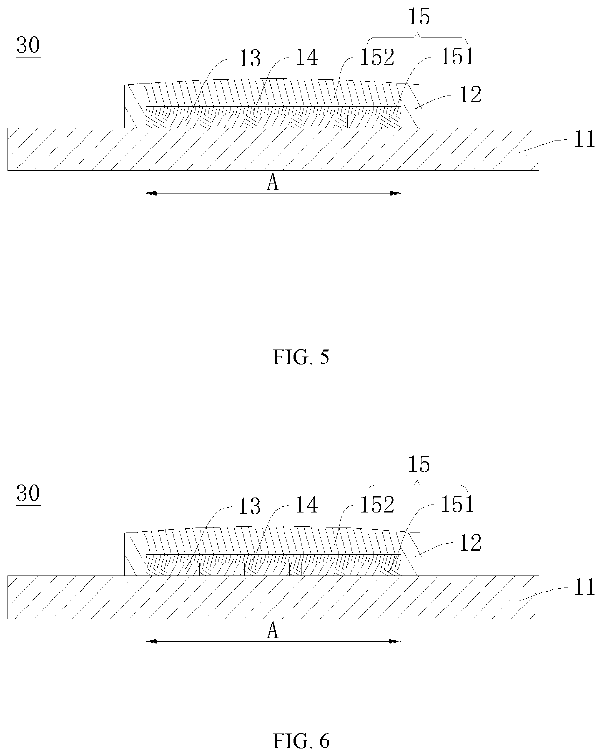
[0054]Referring to FIG. 5, the third embodiment of the disclosure provides a COB type photoelectric device. As shown in FIG. 5, the COB type photoelectric device 30 may include a metallic substrate 11, a dam 12, multiple first photoelectric elements 13, a KSF phosphor based layer 14 and an isolation layer 15.

[0055]The metallic substrate 11 may include a photoelectric element fixing area A. The dam 12 is disposed on the metallic substrate 11 and surrounding the photoelectric element fixing area A. The multiple first photoelectric elements 13 are disposed on the metallic substrate 11 and in the photoelectric element fixing area A. The KSF phosphor based layer 14 is disposed on the multiple first photoelectric elements 13 and being not in contact with the metallic substrate 11. The KSF phosphor based layer 14 includes a KSF phosphor. The isolation layer 15 is disposed in the dam 12 and covering the KSF phosphor based layer 14.

[0056]As shown in FIG. 5, the isolation layer 15 may include...


PUM


Abstract

A COB type photoelectric device is provided. The COB type photoelectric device includes: a metallic substrate including a photoelectric element fixing area; a dam disposed on the metallic substrate and surrounding the photoelectric element fixing area; first photoelectric elements disposed on the metallic substrate and in the photoelectric element fixing area; a KSF phosphor based layer disposed on the first photoelectric elements and being not in contact with the metallic substrate; and an isolation layer disposed in the dam and covering the KSF phosphor based layer. The KSF phosphor based layer includes a KSF phosphor. The COB type photoelectric device can make full use of high luminous efficiency performance of the KSF, and improve luminous efficiency of the COB type photoelectric device while maintaining stability of the KSF.

Description

FIELD OF THE DISCLOSURE[0001]The disclosure relates to the field of photoelectric technologies, and more particularly to a chip-on-board (COB) type photoelectric device.BACKGROUND OF THE DISCLOSURE[0002]Nowadays, LED (light emitting diode) light sources are widely used in displays, lightings, advertising signs and other places due to their high brightness, low power consumption, long service life and simple installation. With the gradual maturity of LED light source technology, its application range is more extensive. At present, one of the mainstream LED light sources in the market is chip-on-board (COB) type light source. During the packaging and manufacturing of an existing COB type light source, a KSF (generally K2SiF6:Me4+) phosphor will be added therein. The KSF phosphor has a relatively high luminous efficiency, and its application in the COB type light source can improve the luminous efficiency of the COB type light source. However, due to KSF material has strong metal corro...

Claims


Application Information

Patent Timeline
IPC IPC(8): H01L33/50H01L27/15H01L33/52
CPCH01L33/502H01L33/52H01L27/156H01L25/0753H01L33/504H01L33/508H01L33/505H01L33/44
Inventor HUANG, DEBINGSHEN, ZHIKUNLI, YIQUNWANG, GANGYUAN, XIANGLONG
Owner KAISTAR LIGHTING (XIAMEN) CO LTD
Why Eureka
Try Eureka