
Semiconductor device, display apparatus, electronic device, and operation method of semiconductor device

a technology of semiconductor devices and display devices, which is applied in the direction of semiconductor devices, electrical devices, instruments, etc., can solve the problems of slowing down the operation of the arithmetic circui

Active Publication Date: 2022-09-15
SEMICON ENERGY LAB CO LTD
View PDF2 Cites 3 Cited by
  • Summary
  • Abstract
  • Description
  • Claims
  • Application Information

AI Technical Summary

Benefits of technology

The present invention provides a semiconductor device with a reduced circuit area and a high driving speed. The device uses an arithmetic circuit that employs analog currents, leading to lower power consumption. However, the low analog current may slow down the operation of the circuit. To address this issue, the invention proposes a multi-gate structure for the transistor, which reduces the off-state current and improves the reliability of the transistor. Additionally, the invention utilizes the flat slope of voltage-current characteristics obtained by the multi-gate structure to achieve an ideal current source circuit or an active load with very high resistance. The invention also discusses the use of a light-emitting device with an SBS structure to achieve lower power consumption and the preferential manufacturing process of a white-light-emitting device for cost-effectiveness or yield improvement.

Problems solved by technology

However, such a low analog current extends the time taken to charge a capacitor, a wiring, an electrode, and the like of the circuit with electric charges and might accordingly slow down the operation of the arithmetic circuit.

Method used


Image

  • Semiconductor device, display apparatus, electronic device, and operation method of semiconductor device
  • Semiconductor device, display apparatus, electronic device, and operation method of semiconductor device
  • Semiconductor device, display apparatus, electronic device, and operation method of semiconductor device

Examples


embodiment 1

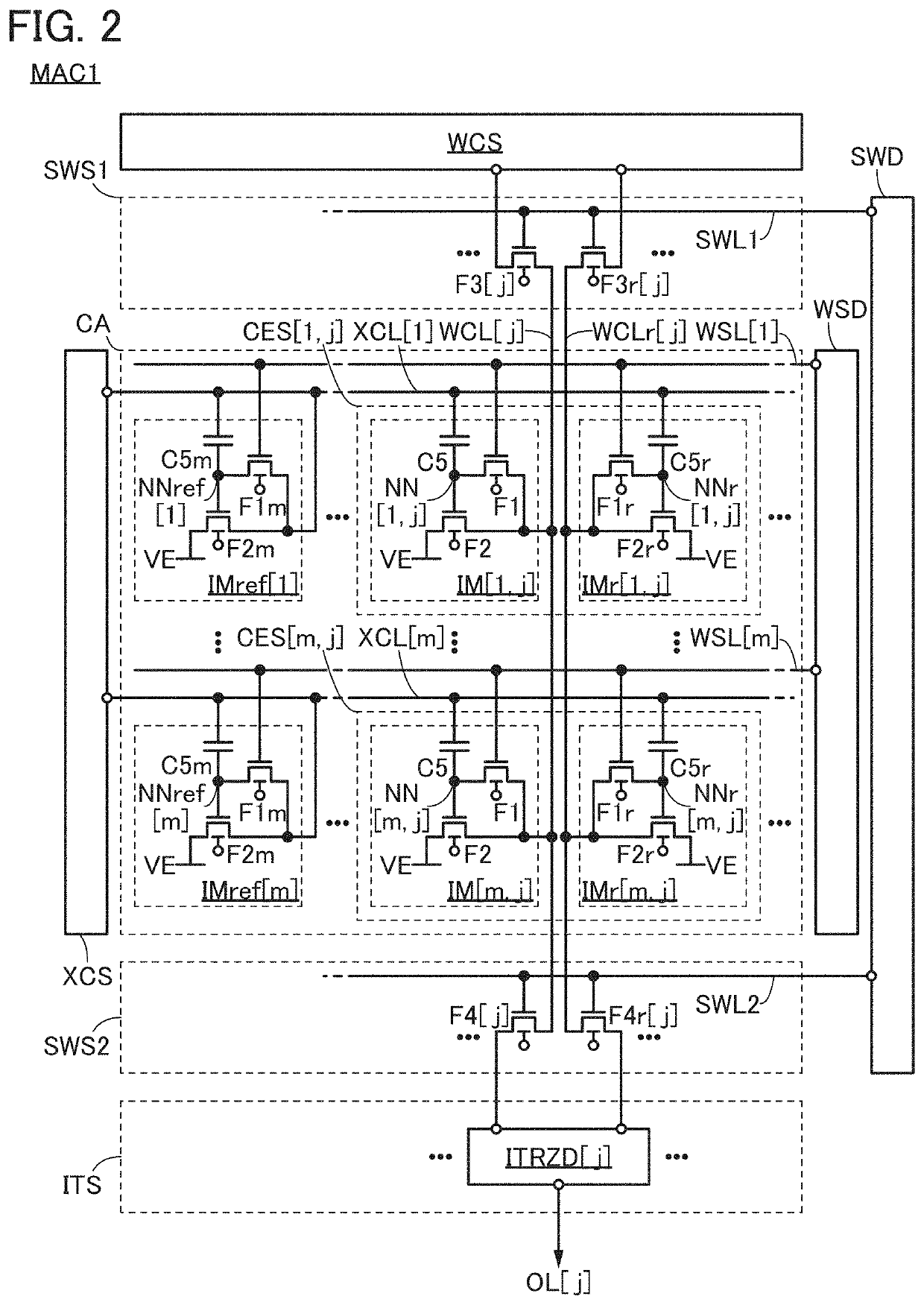
[0126]In this embodiment, an arithmetic circuit which is a semiconductor device of one embodiment of the present invention is described.

[0127]FIG. 2 shows a configuration example of an arithmetic circuit which performs a product-sum operation of positive, negative, or “0” first data and positive or “0” second data. An arithmetic circuit MAC1 illustrated in FIG. 2 performs a product-sum operation of the first data corresponding to a potential stored in each cell and the second data corresponding to an input potential, and performs an arithmetic operation of a function using the result of the product-sum operation. The function can be an activation function in the case where an arithmetic operation in a neural network is performed, for example. Note that the first data and the second data can be, for example, analog data or multilevel data (discrete data).

[0128]The arithmetic circuit MAC1 includes a circuit WCS, a circuit XCS, a circuit WSD, a circuit SWD, a circuit SWS1, a circuit SW...

embodiment 2

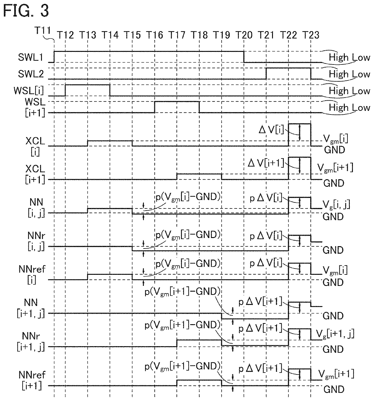
[0322]In this embodiment, examples of operation methods of the arithmetic circuits MAC1, MAC2, and MAC3 that are the semiconductor devices of embodiments of the present invention are described.

[0323]Each of the arithmetic circuits MAC1, MAC2, and MAC3 can perform arithmetic processing through any one of a low-peak-power mode operation (also referred to as first operation), a high-arithmetic-efficiency mode operation (also referred to as second operation), and a high-throughput mode operation (also referred to as third operation).

[0324]In the low-peak-power mode, the power consumption of the arithmetic circuit MAC1, MAC2, or MAC3 is kept low. In the low-peak-power mode, for example, the power consumption of the arithmetic circuit MAC1, MAC2, or MAC3 can be reduced by reducing the amounts of currents flowing in the wirings WCL and WCLr in the arithmetic circuit MAC1, MAC2, or MAC3. In this case, the reduction in the amounts of currents flowing in the wirings WCL and WCLr might reduce ...

embodiment 3

[0383]In this embodiment, the configurations of the circuits included in the arithmetic circuits in the above embodiments are described.

[0384]First, specific examples of the circuit WCS and the circuit XCS shown in FIG. 2 are described.

[0385]First, the circuit WCS is described. FIG. 12A is a block diagram showing an example of the circuit WCS. In FIG. 12A, the circuit SWS1, the transistor F3, the wiring SWL1, and the wiring WCL are illustrated to show the electrical connection between the circuit WCS and its nearby circuits.

[0386]The circuit WCS includes, for example, circuits WCSa the number of which is the same as that of the wirings WCL and WCLr. That is, the circuit WCS includes 2×n circuits WCSa.

[0387]The circuit SWS1 includes the transistors F3 the number of which is the same as that of the wirings WCL. That is, the circuit SWS1 includes n transistors F3. In a similar manner, the circuit SWS1 includes the transistors F3r the number of which is the same as that of the wirings W...

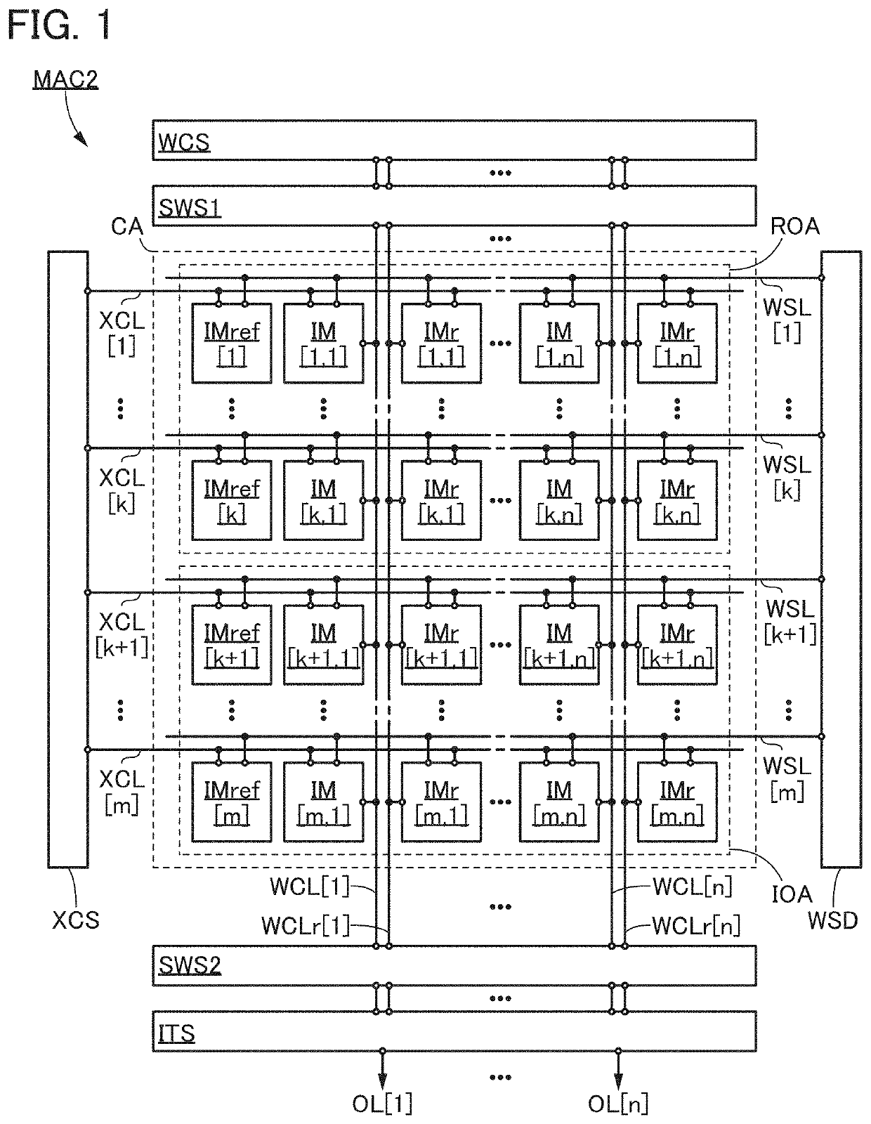

PUM

PropertyMeasurementUnit
resistanceaaaaaaaaaa

Abstract

A semiconductor device with a high driving speed is provided. The semiconductor device includes first to fourth cells, a converter circuit, and first to fourth wirings. The first and second cells make a first current and a second current each corresponding to the product of first data and second data flow in the first wiring and the second wiring, respectively. The third and fourth cells make base currents in the same amount flow in the first and second wirings. The converter circuit outputs, from an output terminal thereof, a voltage corresponding to the differential current between the sum of the first current and the base current flowing in the first wiring and the sum of the second current and the base current flowing in the second wiring.

Description

BACKGROUND OF THE INVENTION1. Field of the Invention[0001]One embodiment of the present invention relates to a semiconductor device, a display apparatus, an electronic device, and an operation method of a semiconductor device.[0002]Note that one embodiment of the present invention is not limited to the above technical field. The technical field of the invention disclosed in this specification and the like relates to an object, a driving method, or a manufacturing method. Alternatively, one embodiment of the present invention relates to a process, a machine, manufacture, or a composition of matter. Therefore, specific examples of the technical field of one embodiment of the present invention disclosed in this specification include a semiconductor device, a display apparatus, a liquid crystal display apparatus, a light-emitting apparatus, a power storage device, an imaging device, a memory device, a signal processing device, a processor, an electronic device, a system, a driving metho...

Claims


Application Information

Patent Timeline
Patent Type & Authority Applications(United States)
IPC IPC(8): G09G3/3208H01L27/32
CPCG09G3/3208H01L27/3262H01L27/3269H01L29/78648G09G2354/00G09G3/20G09G2310/0262G09G2360/142H01L27/1207H01L29/7869H01L27/1225H10K59/13H10K59/1213
Inventor GODO, HIROMICHIKUROKAWA, YOSHIYUKITSUDA, KAZUKIOHSHITA, SATORURIKIMARU, HIDEFUMI
Owner SEMICON ENERGY LAB CO LTD
Learn More