Eureka AIR delivers breakthrough ideas for toughest innovation challenges, trusted by R&D personnel around the world.

Semiconductor IC device and method of manufacturing the same

Pending Publication Date: 2022-11-17
SAMSUNG ELECTRONICS CO LTD
View PDF0 Cites 0 Cited by
  • Summary
  • Abstract
  • Description
  • Claims
  • Application Information

AI Technical Summary

Benefits of technology

This patent involves a method to prevent the inactivation of certain dopants in semiconductor layers. The method involves using two layers of passivation, where the second layer partially inactivates the dopant in the second layer, while the first layer prevents the first layer from inactivating the dopant in the first layer. This technique helps to improve the performance of semiconductor devices.

Problems solved by technology

It may be more and more difficult to increase the efficiency of a silicon (Si)-based power device due to the limitations of the properties of silicon and those of the manufacturing process.

Method used


Image

  • Semiconductor IC device and method of manufacturing the same
  • Semiconductor IC device and method of manufacturing the same
  • Semiconductor IC device and method of manufacturing the same

Examples


Embodiment Construction

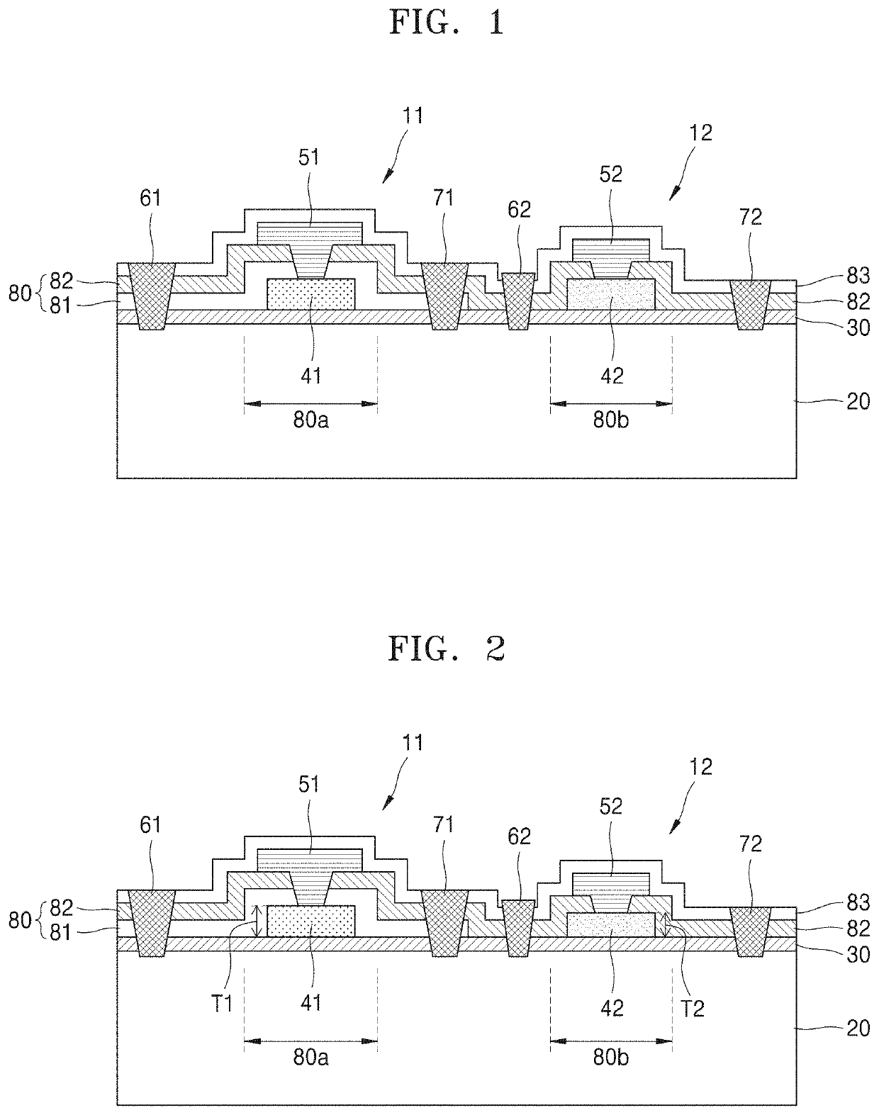
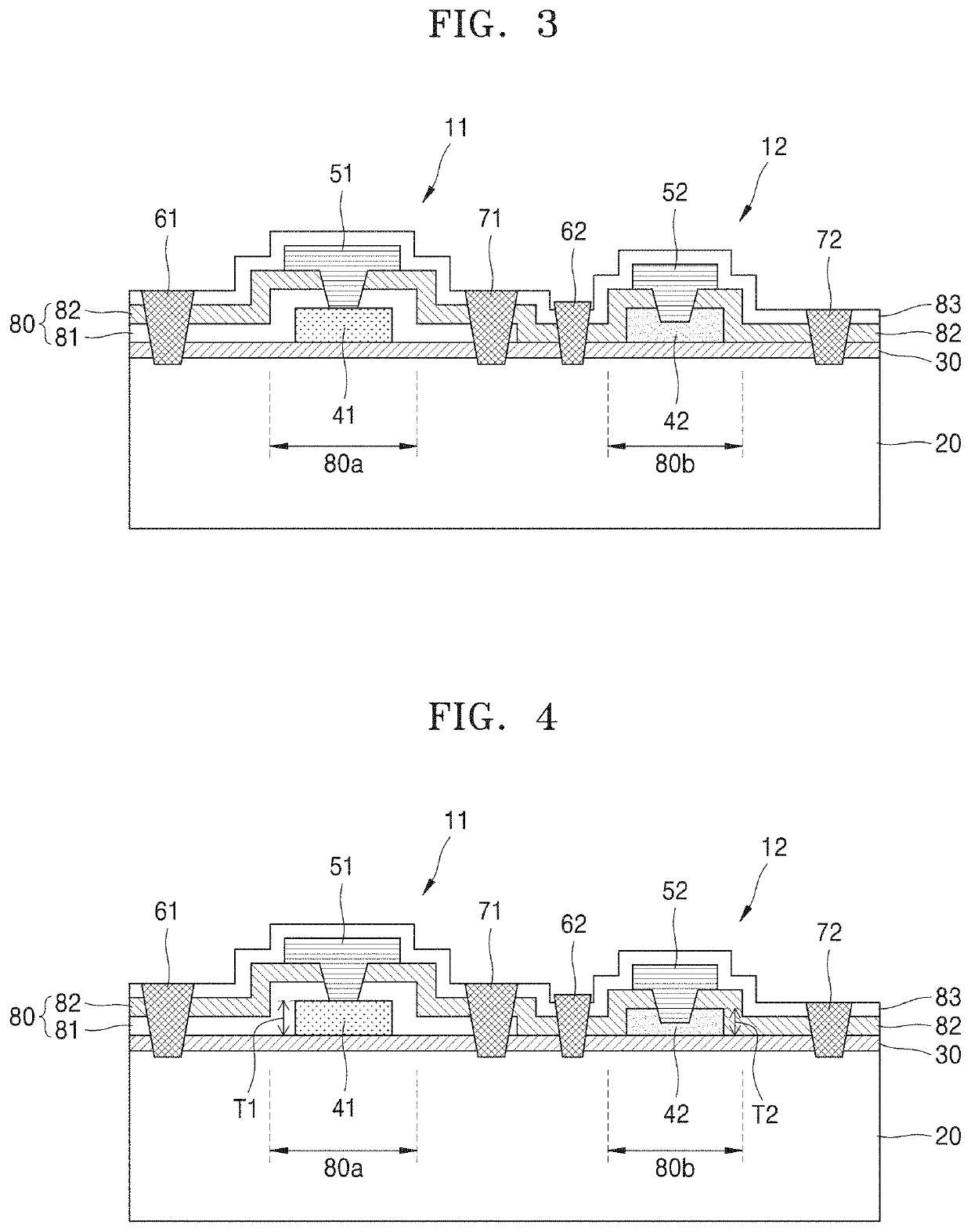
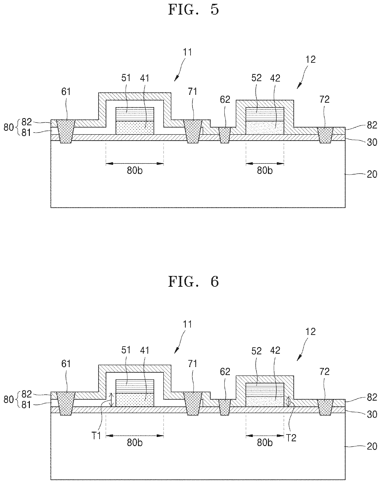
[0049]Reference will now be made in detail to embodiments, examples of which are illustrated in the accompanying drawings, wherein like reference numerals refer to like elements throughout. In this regard, the present embodiments may have different forms and should not be construed as being limited to the descriptions set forth herein. Accordingly, the embodiments are merely described below, by referring to the figures, to explain aspects. As used herein, the term “and / or” includes any and all combinations of one or more of the associated listed items. Expressions such as “at least one of,” when preceding a list of elements, modify the entire list of elements and do not modify the individual elements of the list.

[0050]Hereinafter, embodiments of the present disclosure will be described in detail with reference to the attached drawings. In the drawings, like reference numerals denote like elements, and the sizes of the elements may be exaggerated for clarity and convenience. The embo...


PUM


Abstract

A semiconductor integrated circuit device includes: a channel layer, a barrier layer; a first p-type semiconductor layer and a second p-type semiconductor layer, spaced apart from each other on the barrier layer; and a passivation layer on the first p-type semiconductor layer and the second p-type semiconductor layer. The passivation layer may partially inactivate a dopant of at least one of the first p-type semiconductor layer and the second p-type semiconductor layer.

Description

CROSS-REFERENCE TO RELATED APPLICATION[0001]This application is based on and claims priority under 35 U.S.C. § 119 to Korean Patent Application No. 10-2021-0061645, filed on May 12, 2021, in the Korean Intellectual Property Office, the disclosure of which is incorporated by reference herein in its entirety.BACKGROUND1. Field[0002]The present disclosure relates to semiconductor integrated circuit devices and / or methods of manufacturing the same.2. Description of the Related Art[0003]Various power converting systems may require a device for controlling the flow of current via ON / OFF switching, such as a switching device. In a power converting system, the efficiency of a switching device may decide the efficiency of the entire system.[0004]It may be more and more difficult to increase the efficiency of a silicon (Si)-based power device due to the limitations of the properties of silicon and those of the manufacturing process. To overcome these limitations, research and development into...

Claims


Application Information

Patent Timeline
IPC IPC(8): H01L29/778H01L29/20H01L29/66
CPCH01L29/7786H01L29/2003H01L29/66431H01L27/085H01L21/8232H01L29/1029H01L29/778H01L29/1066H01L21/8252H01L27/0605H01L27/098H01L23/3171H01L29/41766H01L29/42316H01L29/66462H01L23/3192H01L29/207H01L29/4236
Inventor HWANG, SUNKYUKIM, JONGSEOBKIM, JOONYONGPARK, YOUNGHWANPARK, JUNHYUKOH, JAEJOONHWANG, INJUN
Owner SAMSUNG ELECTRONICS CO LTD
Why Eureka
Eureka Blog
Learn More