Method for etching silicon oxynitride and inorganic antireflection coatings

a technology of inorganic antireflection coating and silicon oxynitride, which is applied in the direction of decorative surface effects, electrical equipment, decorative arts, etc., can solve the problem of lowering the productivity of the whole process

Inactive Publication Date: 2000-01-11
APPLIED MATERIALS INC
View PDF22 Cites 99 Cited by
  • Summary
  • Abstract
  • Description
  • Claims
  • Application Information

AI Technical Summary

Problems solved by technology

However, as silicon oxynitride is a dielectric material, its patterning is traditionally reserved for dielectric etch chambers, and moving the substrate from one process chamber to another l

Method used


Image

  • Method for etching silicon oxynitride and inorganic antireflection coatings
  • Method for etching silicon oxynitride and inorganic antireflection coatings
  • Method for etching silicon oxynitride and inorganic antireflection coatings

Examples


example two

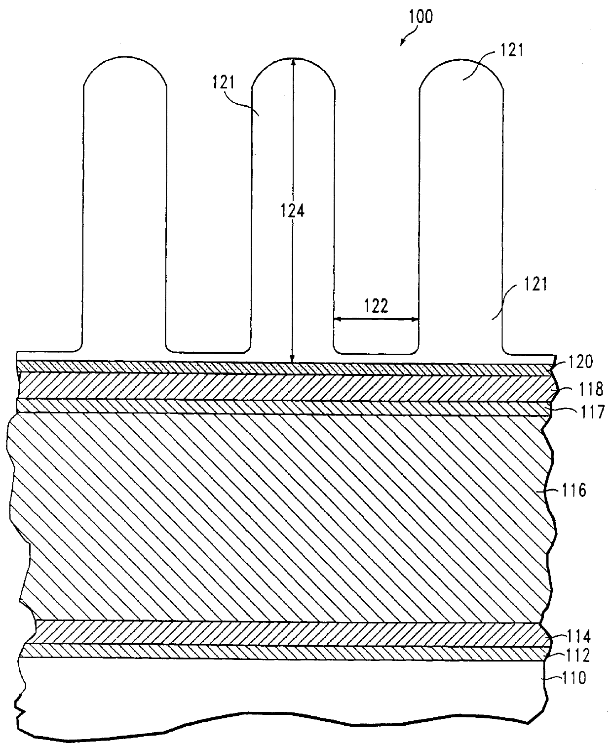
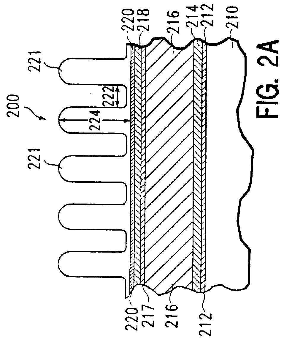
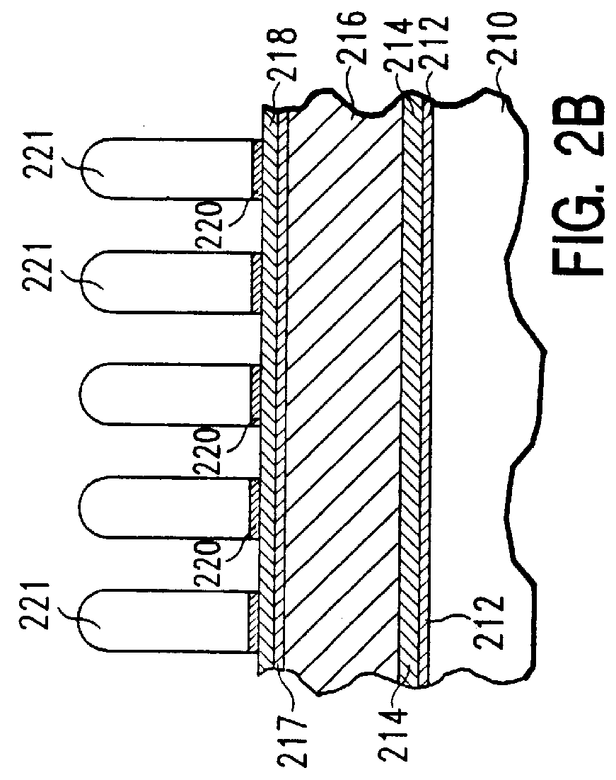
This Example is for a two step etch in which the SiO.sub.x N.sub.y ARC layer and the underlying titanium nitride and titanium barrier layers, are etched in Step 1; and, the aluminum layer, and titanium nitride and titanium layers which underlie the aluminum layer are etched in Step 2. With reference to FIGS. 3A through 3C, FIG. 3A illustrates the schematic cross-sectional profile of the preferred embodiment stack 300 (the same stack as 100 described with reference to FIG. 1) for the two etch steps.

FIG. 3B shows the schematic of the cross-sectional profile of the etch stack after the first etch step in which the pattern is transferred from DUV photoresist layer 321 through silicon oxynitride layer 320, second titanium nitride barrier layer 318, and second titanium layer 317, stopping at the upper surface of aluminum layer 316. The etch conditions used to carry out this first etch step were as follows. The source power was 1400 W; the bias power was 70 W; the process chamber pressure ...


PUM

PropertyMeasurementUnit
Lengthaaaaaaaaaa
Timeaaaaaaaaaa
Timeaaaaaaaaaa

Abstract

The present disclosure pertains to a method for plasma etching a semiconductor patterning stack. The patterning stack includes at least one layer comprising either a dielectric-comprising antireflective material or an oxygen-comprising material. In many instances the dielectric-comprising antireflective material will be an oxygen-comprising material, but it need not be limited to such materials. In one preferred embodiment of the method, the chemistry enables the plasma etching of both a layer of the dielectric-comprising antireflective material or oxygen-comprising material and an adjacent or underlying layer of material. In another preferred embodiment of the method, the layer of dielectric-comprising antireflective material or oxygen-comprising material is etched using one chemistry, while the adjacent or underlying layer is etched using another chemistry, but in the same process chamber. Of particular interest is silicon oxynitride, an oxygen-comprising material which functions as an antireflective material. A preferred embodiment of the method provides for the use of a source of carbon and an appropriate halogen-comprising plasma, to achieve selective etch of one oxygen-containing material compared with another material which contains a more limited amount of oxygen.

Description

1. Field of the InventionThe present invention pertains to a method of etching silicon oxynitride and other oxygen containing materials. In addition, the method is applicable to inorganic antireflective coating (ARC) materials. Silicon oxynitride is commonly used as an antireflective coating in combination with deep ultraviolet (DUV) photoresists.2. Brief Description of the Background ArtIn the field of semiconductor device fabrication, DUV photoresists have been developed which take advantage of shorter wavelengths of ultraviolet radiation to enable the patterning of smaller-dimensioned electronic and optical devices than possible with traditional, or so called I-line photoresists.. Generally, the photoresist is applied over a stack of layers of various materials to be patterned in subsequent processing steps. Some of the layers in the stack are consumed during the process of patterning underlying layers which become part of the functioning device. To take advantage of the spacial ...

Claims


Application Information

Patent Timeline
IPC IPC(8): H01L21/027H01L21/02H01L21/3213H01L21/302H01L21/3065
CPCH01L21/0276H01L21/32139
Inventor IONOV, PAVELKIM, SUNG HOLI, DEAN
Owner APPLIED MATERIALS INC
Why Eureka
Try Eureka