Method and apparatus for in-line oxide thickness determination in chemical-mechanical polishing

a technology of in-line oxide thickness and polishing method, which is applied in the direction of semiconductor/solid-state device testing/measurement, coating machines, instruments, etc., can solve the problems of inability to determine the thickness or endpoint of a required thickness, highly undesirable, and the method is extremely time-consuming

Inactive Publication Date: 2000-02-01
IBM CORP
View PDF12 Cites 147 Cited by
  • Summary
  • Abstract
  • Description
  • Claims
  • Application Information

AI Technical Summary

Problems solved by technology

A persistent difficulty in the fabrication of VLSI wafers is the inability to determine when a required thickness or endpoint has been reached during a dielectric polishing step. one method of determining the required thickness or CMP endpoint is by using estimated CMP rates and times. CMP rates vary considerably with time however, due to changes in polishing pad characteristics, for example.
With ex-situ thickness measurements, the method is extremely time consuming and highly undesirable since operators must handle, unload, and dry each wafer after polish before making the ex-situ thickness measurement.

Method used


Image

  • Method and apparatus for in-line oxide thickness determination in chemical-mechanical polishing
  • Method and apparatus for in-line oxide thickness determination in chemical-mechanical polishing
  • Method and apparatus for in-line oxide thickness determination in chemical-mechanical polishing

Examples


Embodiment Construction

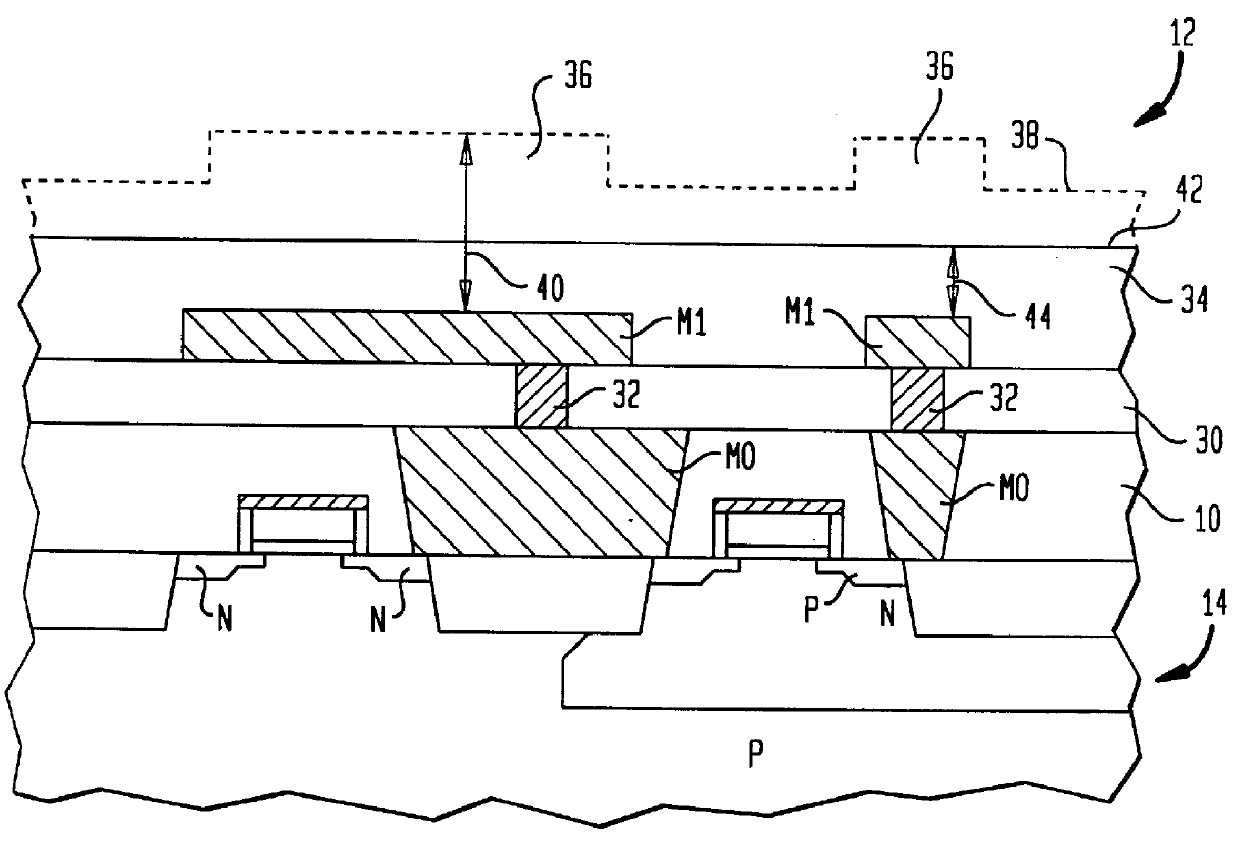
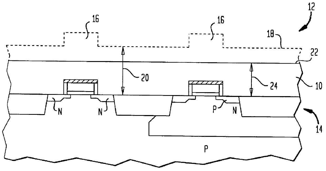
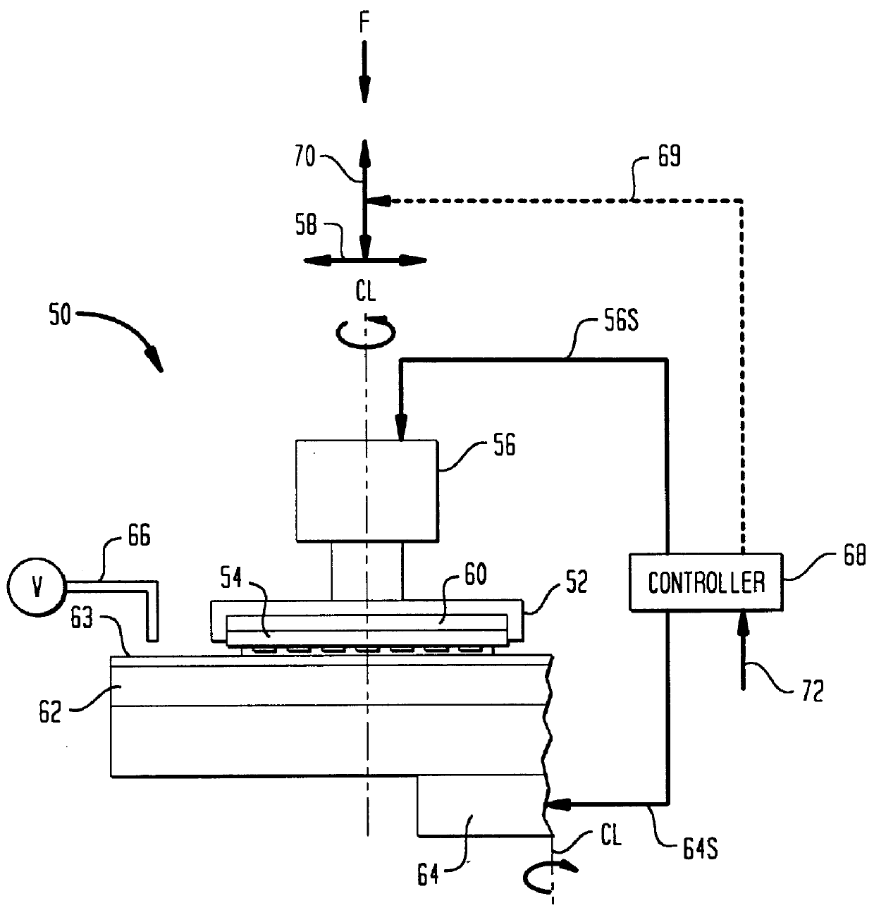
Referring now to FIG. 3, an apparatus suitable for performing a chemical mechanical planarization (CMP) process in accordance with the present invention is shown and generally designated by numeral 50. The chemical mechanical planarization apparatus 50 includes a wafer carrier 52 for holding a semiconductor wafer 54. The wafer carrier 52 is mounted for rotation as desired by a drive motor 56. In addition, the wafer carrier 52 is mounted for transverse movement as desired, further as indicated by the double headed arrow 58. The wafer carrier 52 may also include a wafer carrier pad 60 formed of a soft material for contacting a backside of the wafer 54. Additionally, wafer carrier 52 may further include a vacuum holding means (not shown) for holding the wafer 54 in the wafer carrier 52 during the chemical mechanical planarization process. The wafer carrier 52 is still further adapted for exerting a downward force F upon the wafer 54. The CMP apparatus 50 further includes a polishing pl...


PUM

PropertyMeasurementUnit
voltageaaaaaaaaaa
frequenciesaaaaaaaaaa
thicknessaaaaaaaaaa

Abstract

In-line thickness measurement of a dielectric film layer on a surface of a workpiece subsequent to a polishing on a chemical-mechanical polishing machine in a polishing slurry is disclosed. The workpiece includes a given level of back-end-of-line (BEOL) structure including junctions. The measurement apparatus includes a platen and an electrode embedded within the platen. A positioning mechanism positions the workpiece above the electrode with the dielectric layer facing in a direction of the electrode. A slurry dam is used for maintaining a prescribed level of a conductive polishing slurry above the electrode, the prescribed level to ensure a desired slurry coverage of the workpiece. A capacitance sensor senses a system capacitance C in accordance with an RC equivalent circuit model, wherein the RC equivalent circuit includes a resistance R representative of the slurry and workpiece resistances and the system capacitance C representative of the dielectric material and junction capacitances. Lastly, a capacitance-to-thickness converter converts the sensed capacitance to a dielectric thickness in accordance with a prescribed system capacitance / optical thickness calibration, wherein the prescribed calibration corresponds to the given level of BEOL structure of the workpiece.

Description

1. Field of the InventionThis invention relates generally to chemical mechanical planarization or polishing tools and, more particularly, to a method and apparatus of in-line oxide thickness determination subsequent to chemical mechanical polishing of a semiconductor wafer.2. Discussion of the Related ArtIn semiconductor device manufacturing of very large scale integrated (VLSI) circuits, extremely small electronic devices are formed in separate dies on a thin, flat semiconductor wafer. In general, various materials which are either conductive, insulating, or semiconducting are utilized in the fabrication of integrated circuitry on semiconductor wafers. These materials are patterned, doped with impurities, or deposited in layers by various processes to form integrated circuits. VLSI integrated circuits include patterned metal layers which are generally covered with dielectric materials, such as oxide, followed by a subsequent metalization, etc. The semiconductor wafers thus contain ...

Claims


Application Information

Patent Timeline
Patent Type & Authority Patents(United States)
IPC IPC(8): B24B37/04B24B49/04B24B49/02H01L21/66H01L21/02H01L21/3105G01B7/06B24B37/013G01N27/22H01L21/304
CPCB24B37/013B24B49/04G01B7/085H01L21/31053H01L22/20H01L22/12H01L22/00
Inventor LUSTIG, NAFTALI ELIAHUGUTHRIE, WILLIAM L.SANDWICK, THOMAS E.
Owner IBM CORP
Why Eureka
Try Eureka