System and method for inspecting semiconductor wafers

Inactive Publication Date: 2000-02-01
KLA TENCOR CORP
View PDF5 Cites 221 Cited by
  • Summary
  • Abstract
  • Description
  • Claims
  • Application Information

AI Technical Summary

Benefits of technology

The present invention addresses the problem by providing a high-throughput inspection system at low cost, particularly for equipment monitoring applications. A single low-cost unit can be provided using "consumer grade" devices for illumination, imaging, image sensing, and image-processing which can measure a part of the wafer by itself with acceptable sensitivity, and with very high speed. A system can be provided utilizing a plurality of single units which can be scanned over t

Problems solved by technology

Consequently, expensive special-purpose optical, mechanical, electronic, and computer processing systems have been employed in state-of-the-art tools.
For example, these systems may allow adjustments in magnification l

Method used


Image

  • System and method for inspecting semiconductor wafers
  • System and method for inspecting semiconductor wafers
  • System and method for inspecting semiconductor wafers

Examples


Embodiment Construction

Presently, preferred wafer-inspection systems, in accordance with the present invention, will be described below making, reference to the accompanying drawings. It should be understood that the invention is not limited to these embodiments which are provided to present certain aspects and examples of the invention. It should be understood that while the methods and apparatus presented herein cover systems for imaging a patterned semiconductor wafer, they could also be employed to image rough films, unpatterned semiconductor wafers, backsides of wafers, photomasks, reticles, flat panel displays such as LCDs, etc.

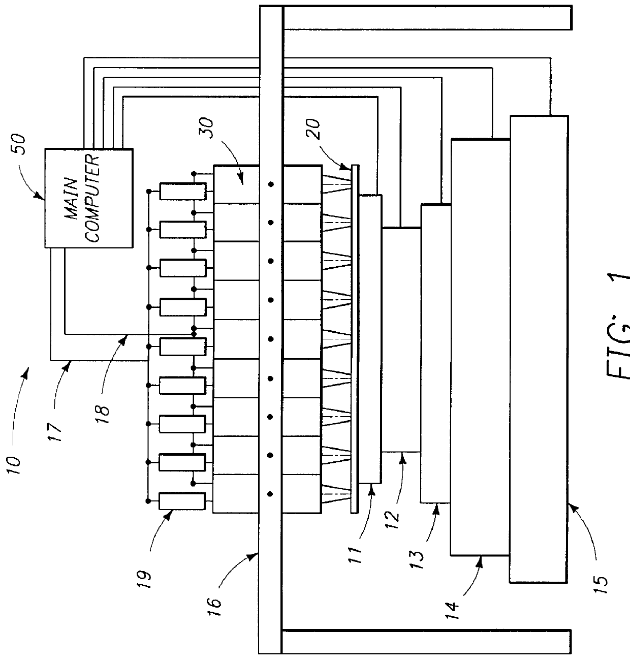
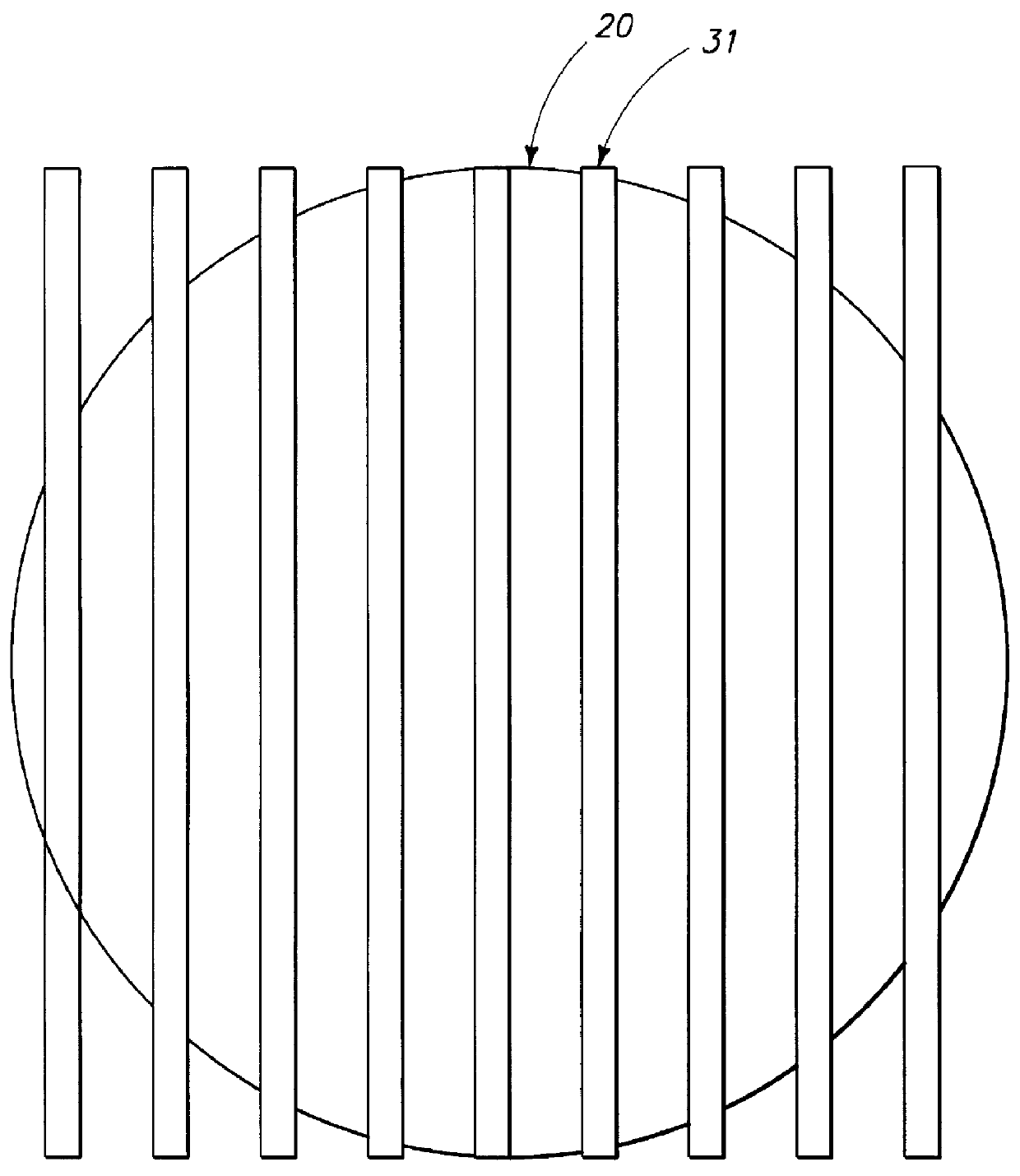
FIG. 1 shows a block diagram of a system 10 of a preferred embodiment of the present invention. System 10 includes a plurality of imaging subsystems 30. The imaging subsystems 30 work in parallel, each simultaneously analyzing a portion of a wafer 20. The imaging subsystems 30 are kinematically supported over wafer 20 by a supporting structure 16. As portions the length of th...


PUM


Abstract

A method for inspecting semiconductor wafers is provided in which a plurality of independent, low-cost, optical-inspection subsystems are packaged and integrated to simultaneously perform parallel inspections of portions of the wafer, the wafer location relative to the inspection being controlled so that the entire wafer is imaged by the system of optical subsystems in a raster-scan mode. A monochromatic coherent-light source illuminates the wafer surface. A darkfield-optical system collects scattered light and filters patterns produced by valid periodic wafer structures using Fourier filtering. The filtered light is processed by general purpose digital-signal processors. Image subtraction methods are used to detect wafer defects, which are reported to a main computer to aid in statistical process control, particularly for manufacturing equipment.

Description

BACKGROUND OF THE INVENTIONThis application relates to an apparatus and method for optical inspection of semiconductor wafers. In particular, the apparatus and method of the present invention provide high-throughput inspection of wafers using a plurality of independent good sensitivity, low-cost inspection devices whose packaging and form factor allow operation in parallel. The present invention may be applied to brightfield and / or darkfield inspection systems.Optical inspection of semiconductor wafers has become a standard step in the production of semiconductors. Wafers are illuminated with light emanating from a controlled illuminator, and an image of the surface is constructed based on the portion of the light reflected or otherwise directed to a light sensor. The image is processed to isolate defects from valid structures.The sensitivity of optical inspection systems to small sized defects on a patterned wafer surface is determined by the ability of the system to discriminate b...

Claims


Application Information

Patent Timeline
IPC IPC(8): G01N21/95G01N21/88G01N21/956G01B11/30G06T1/00H01L21/66H01L21/677
CPCG01N21/9501G01N21/95623H01L21/67155G01N2021/8822
Inventor ROSENGAUS, ELIEZERLANGE, STEVEN R.
Owner KLA TENCOR CORP
Why Eureka
Try Eureka