Method of cleaning and treating a semiconductor device including a micromechanical device

a micromechanical device and cleaning technology, applied in the direction of cleaning using liquids, instruments, optical elements, etc., can solve the problems of reducing device reliability, preventing a suitable deposition of a passivation layer, and degrading the effectiveness of the subsequent passivation step

Inactive Publication Date: 2000-02-15
TEXAS INSTR INC
View PDF22 Cites 186 Cited by
  • Summary
  • Abstract
  • Description
  • Claims
  • Application Information

AI Technical Summary

Problems solved by technology

If the cleaned surface is not maintained in the SCF chamber, contamination from organics and inorganics that reside in even a Class-1 clean room can preclude a suitable deposition of a passivation layer.
Should device 10 not be maintained within the sealed SCF chamber, such as being transported through the ambient of a level one clean room, the exposed surfaces could be contaminated with molecular level impurities thus degrading the effectiveness of the subsequent passivation step, and reducing device reliability.
Again, it is simply not enough to maintain the device in a clean room during transportation to a separate passivating apparatus if good performance of the device is to be expected over a significant time period.
If the semiconductor wafer is not maintained within the SCF chamber, the quality of the thin gate oxide interface is degraded and may be even totally unsuitable to be further processed, such as subsequent deposition steps, if the gate oxide layer is only about 30 Angstroms in thickness.

Method used


Image

  • Method of cleaning and treating a semiconductor device including a micromechanical device
  • Method of cleaning and treating a semiconductor device including a micromechanical device
  • Method of cleaning and treating a semiconductor device including a micromechanical device

Examples


Embodiment Construction

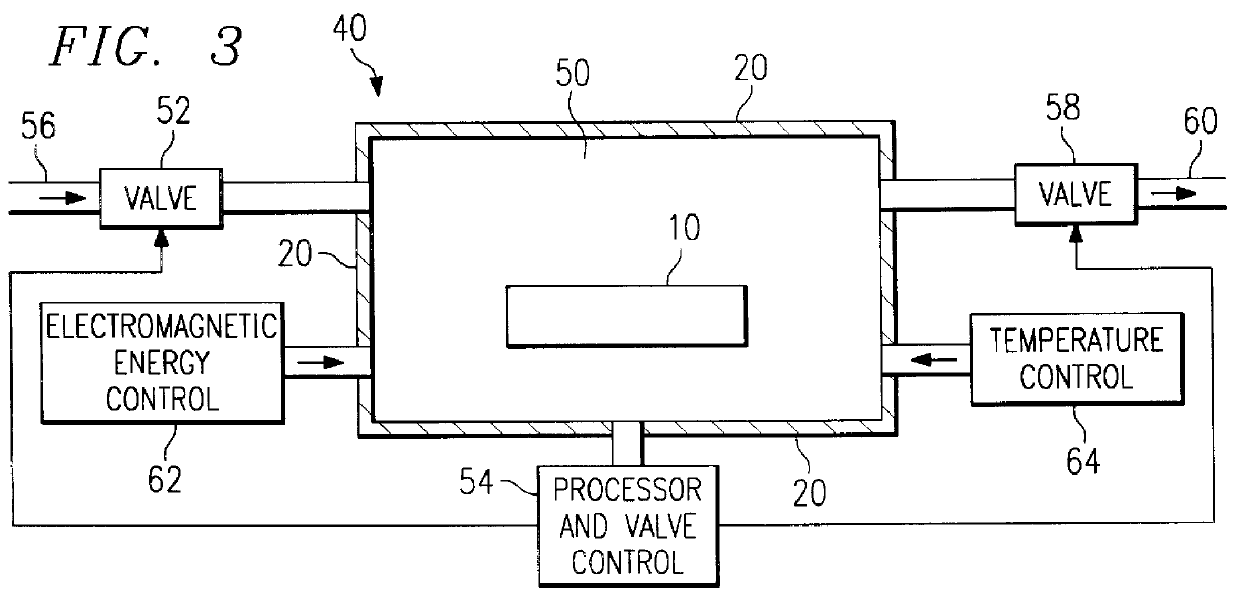
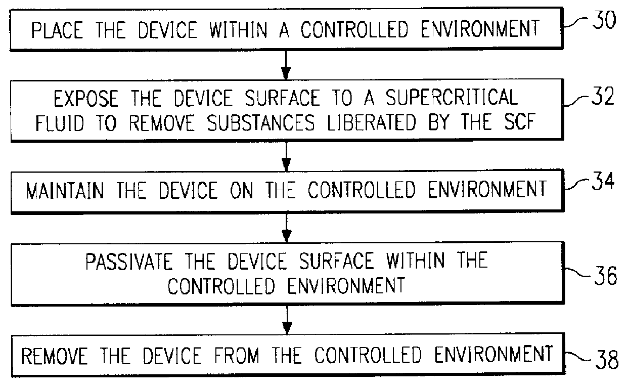
By way of illustration, but without any limitation to, the preferred embodiment of the present invention will be set forth in reference to cleaning and passivating the landing electrode of a bistable digital micromirror device (DMD) spatial light modulator, such as that shown in FIG. 1. However, it is to be understood that the method of the present invention is suitable to clean and passivate other surfaces including, but without limitation to, a semiconductor wafer, or a hard disk of a disk drive.

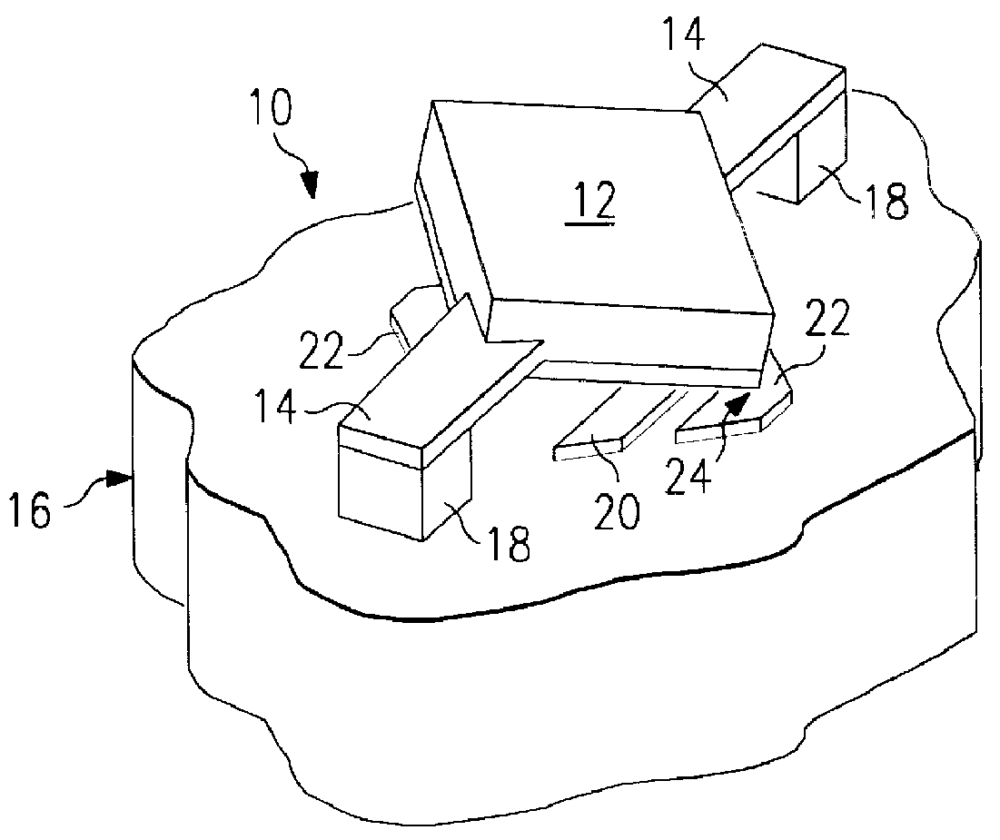
Referring to FIG. 1, a digital micromirror device (DMD) comprising one pixel is generally shown at 10. When used as a spatial light modulator, pixel 10 comprises of one of thousands such pixels arranged in a linear or area array to modulate incident light and generate an image, as set forth in the several cross referenced commonly assigned patents previously discussed in a section entitled Background of the Invention.

Pixel 10 is seen to include a beam comprising a mirror 12 supported by a ...


PUM

PropertyMeasurementUnit
thicknessaaaaaaaaaa
densityaaaaaaaaaa
pressureaaaaaaaaaa

Abstract

A method of cleaning and treating a device, including those of the micromechanical (10) and semiconductor type. The surface of a device, such as the landing electrode (22) of a digital micromirror device (10), is first cleaned with a supercritical fluid (SCF) in a chamber (50) to remove soluble chemical compounds, and then maintained in the SCF chamber until and during the subsequent passivation step. Passivants including PFDA and PFPE are suitable for the present invention. By maintaining the device in the SCF chamber, and without exposing the device to, for instance, the ambient of a clean room, organic and inorganic contaminants cannot be deposited upon the cleaned surface prior to the passivation step. The present invention derives technical advantages by providing an improved passivated surface that is suited to extend the useful operation life of devices, including those of the micromechanical type, reducing stiction forces between contacting elements such as a mirror and its landing electrode. The present invention is also suitable for cleaning and passivating other surfaces including a surface of semiconductor wafers, and the surface of a hard disk memory drive.

Description

REFERENCE TO RELATED APPLICATIONSThe present invention relates generally to cleaning and treating a semiconductor surface, and more particularly, to a method of cleaning and passivating a micromechanical device including a digital micromirror device (DMD) spatial light modulator (SLM).Cleaning and passivating semiconductor surfaces, including those of the micromechanical-type, is difficult due to their architectures which may comprise spatially-convoluted, micron / submicron-scale features. A recent innovation of Texas Instruments Incorporated of Dallas, Tex. is the digital micromirror device or the deformable mirror device (collectively DMD). The DMD is an electro / mechanical / optical Spatial Light Modulator (SLM) suitable for use in displays, projectors and hard copy printers. The DMD is a monolithic single-chip integrated circuit SLM, comprised of a high density area or linear array of 16 micron square deflectable micromirrors on 17 micron centers. These mirrors are fabricated over a...

Claims


Application Information

Patent Timeline
Patent Type & Authority Patents(United States)
IPC IPC(8): B08B7/00B81B3/00B81C1/00G02B26/08H01L21/304
CPCB08B7/00B08B7/0021B81B3/0005B81C1/00857B81C1/0096G02B26/0841B81C2201/112B81C2201/117
Inventor WALLACE, ROBERT M.DOUGLAS, MONTE A.
Owner TEXAS INSTR INC
Why Eureka
Try Eureka