Electrical conductors formed from mixtures of metal powders and metallo-organic decomposition compounds

a technology of metallo-organic decomposition compounds and electrical conductors, which is applied in the direction of non-metal conductors, conductors, metal/alloy conductors, etc., can solve the problems of high curing temperature, difficult handling, and generation of hazardous wastes, and achieve high electrical conductivity with a low curing temperatur

Inactive Publication Date: 2000-03-14
PARELEC
View PDF22 Cites 331 Cited by
  • Summary
  • Abstract
  • Description
  • Claims
  • Application Information

AI Technical Summary

Problems solved by technology

At each of these stages there is opportunity for error, and hazardous wastes are generated in many of the processes.
The latter are the most difficult to handle because of the presence of formaldehyde reducing agent, a known carcinogen, as well as the toxic heavy metals.
The primary problem in the industry is the requirement for high electrical conductivity with a low enough curing temperature to be compatible with the polymer-based circuit boards.
These small, expensive and specialized substrates can withstand the required thick film ink firing temperatures of more than 650.degree. C. and usually above 850.degree. C.
The use of inorganic glass powder binders which are universally used in conventional thick film inks is not possible in this application because none of them melt at a low enough temperature, and the glass will not bond to the metal or to the polymer substrates.
The problem with this approach is that the inks conduct by random contacts between powder grains in the organic matrix, and the conductivity is poor.
However, this patent does not address the problem of obtaining electrical conductivity comparable to bulk metal.
Images of satisfactory resolution (0.003 inches or 75 microns) were obtained, but the conductivity was low because of the extremely small thickness of the layers after decomposition which was less than a micron.
Again, the difficulty was that they were very thin and had inadequate conductivity.
The MOD compound melts before decomposing and spreads over the surface uncontrollably.
Since melting provides for a well-consolidated metal deposit after decomposition, which is desirable, and since some MOD compounds are actually liquids at room temperature, this is an unavoidable problem.
However, the above described thin films alone cannot provide adequate conductivity.

Method used


Image

  • Electrical conductors formed from mixtures of metal powders and metallo-organic decomposition compounds
  • Electrical conductors formed from mixtures of metal powders and metallo-organic decomposition compounds
  • Electrical conductors formed from mixtures of metal powders and metallo-organic decomposition compounds

Examples


example i

A composition, labeled Ink B-2, was formed from the following mixture:

The constituents were blended by hand and screened onto a conventional 0.062 inch thick FR-4 epoxy-glass circuit board substrates. The samples were heated in a stationary oven for twenty minutes at a temperature measured as 185.degree. C. This temperature could have been up to fifty degrees higher based on subsequent measurements.

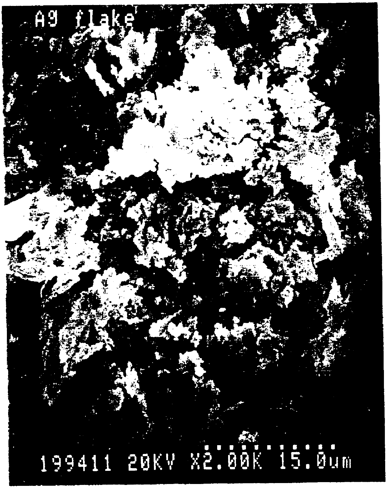
After heating, the MOD compound had completely decomposed leaving a well-defined and well-bonded image with a measured thickness of 0.0006 inches (15 microns). Scotch Tape, Commercial Office Supply Division / 3M. St. Paul, Minn., was applied to the image for removal of silver flake. The measured thickness of the bonded image was reduced to 0.0003 inches. The electrical resistance of the trace measured on a pattern with a width of 0.4 mm and a length of 1.25 meters (3200 squares) was 115 ohms, corresponding to a resistivity of 54 microhm cm. A SEM photograph of composition 1 is shown in FIG....

example ii

A composition labeled Ink B-33 was formed from the following mixture:

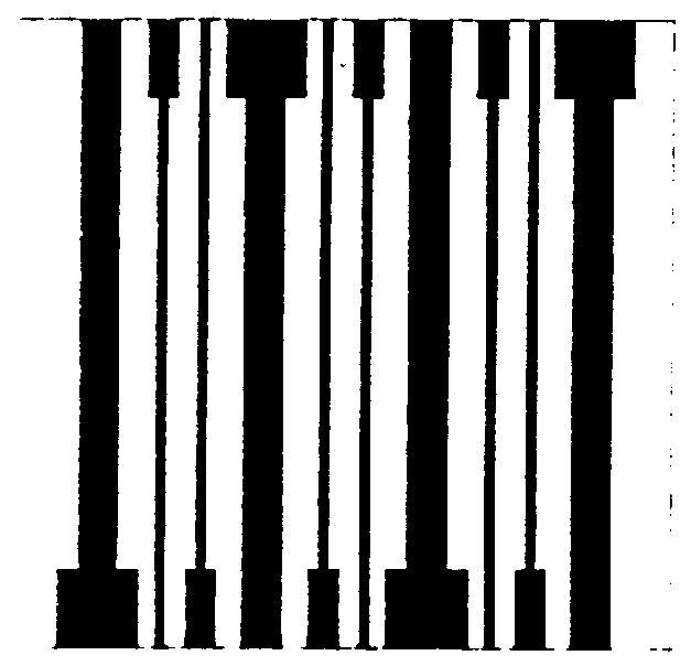
The constituents were weighed out under dry nitrogen and blended in the roll mill. Images were screened onto a DuPont Kapton FN 929 substrate with a semiautomatic screen printer and heated in a stationary oven as before, but with better temperature measurement and at successively higher temperatures. By this technique it was found that there is a critical temperature above which the metal consolidates to a nearly solid form, shown in the SEM cross section of FIG. 4. The sample is inclined with the Kapton substrate at 14, the surface of the silver deposit at 16, the edge of the silver at 18, and a cross-section of the deposit showing the degree of consolidation at 20. The measured electrical resistivities of the test conductors are shown as a function of maximum oven temperature in FIG. 5. Duplicate samples were heated in a stationary oven in air, and the two resistivity values are plotted as solid and hollow square...

example iii

By adding an even finer colloidal silver with a mean particle diameter of approximately 20 nanometers it has been found possible to lower the temperature for consolidating the metal still further to 270.degree. C., as shown in the following example.

A composition labelled Ink B-45 was formed from the following mixture:

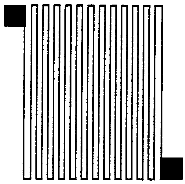
The ingredients were weighed out and mixed under dry, high purity nitrogen. The mixture was blended for fifteen minutes in a two roll mill to prepare a smooth, uniform ink. The ink was screen printed to produce a final thickness of silver of 10-15 microns on samples of DuPont Kapton 300 FN 929. The printed pattern was a conductivity test pattern with a line width of 0.4 mm and a length of 1.25 m (3200 squares).

Three tests for mechanical properties were also performed on the samples.

1) A mandrel test in which the sample was bent around a 1 / 8 inch mandrel.

2) A tape test in which tape was pressed down on the sample.

3) A crease test in which a 180.degree. crease was formed ...


PUM

PropertyMeasurementUnit
aspect ratioaaaaaaaaaa

Abstract

The present invention relates to a thick film formed of a mixture of metal powders and metallo-organic decomposition (MOD) compounds in an organic liquid vehicle and a process for advantageously applying them to a substrate by silk screening or other printing technology. The mixtures preferably contain metal flake with a ratio of the maximum dimension to the minimum dimension of between 5 and 50. The vehicle may include a colloidal metal powder with a diameter of about 10 to about 40 nanometers. The concentration of the colloidal metal in the suspension can range from about 10 to about 50% by weight. The MOD compound begins to decompose at a temperature of approximately about 200 DEG C. to promote consolidation of the metal constituents and bonding to the substrate which is complete at temperatures less than 450 DEG C. in a time less than six minutes. The mixtures can be applied by silk screening, stencilling, gravure or lithography to a polymer-based circuit board substrate for producing rigid and flexible printed wiring boards in a single operation with negligible generation of hazardous wastes. The same mixtures can be used in place of solder to assemble circuits by bonding electrical components to conductors as well as to make the conductors themselves.

Description

1. Field of the InventionThis invention relates to electronic circuits and particularly to printed circuits on conventional polymer-based substrates.2. Description of the Related ArtPrinted circuits are universally used to interconnect and "package" active and passive electronic components to perform a myriad of useful functions. These circuits can be of the rigid type which consist of laminated "boards" usually of glass-reinforced epoxy, but also of paper-phenolic and other constructions. There are also flexible circuits based on unreinforced polymer films such as Kapton polyamide manufactured by DuPont. In both cases the circuits are produced by a combination of etching and deposition technologies based on the use of photoresists which are exposed to light and developed to permit a pattern of conductors to be etched and / or plated on the substrate.These conventional processes are described, for example, in "Printed Circuit Board Basics", M. Flatt, Miller Freeman, San Francisco, 199...

Claims


Application Information

Patent Timeline
Patent Type & Authority Patents(United States)
IPC IPC(8): H01L21/48H01B1/02H01L21/02H01L23/48H01L23/498H05K1/09
CPCH01B1/02H01L21/4867H01L23/49883H05K1/097Y10S977/891H01L2924/0002H01L2924/00
Inventor KYDD, PAUL H.
Owner PARELEC
Why Eureka
Try Eureka