Auto-programmable current limiter to control current leakage due to bitline to wordline short

Inactive Publication Date: 2000-04-11
IBM CORP
View PDF13 Cites 26 Cited by
  • Summary
  • Abstract
  • Description
  • Claims
  • Application Information

AI Technical Summary

Problems solved by technology
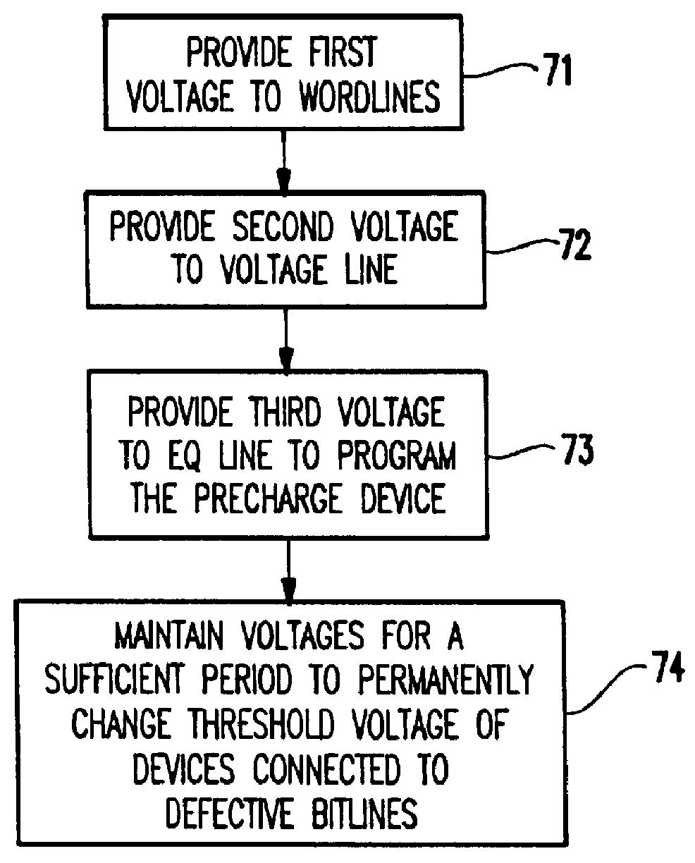
Undesirably large current may be drawn from the voltage supply to ground when a cross fail occurs.
However, the introduction of the depletion device 14, as shown in FIG. 1, increases the chip area and process complexity.
Additionally, the depletion device itself often degrades performance during the array precha

Method used


Image

  • Auto-programmable current limiter to control current leakage due to bitline to wordline short
  • Auto-programmable current limiter to control current leakage due to bitline to wordline short
  • Auto-programmable current limiter to control current leakage due to bitline to wordline short

Examples


first embodiment

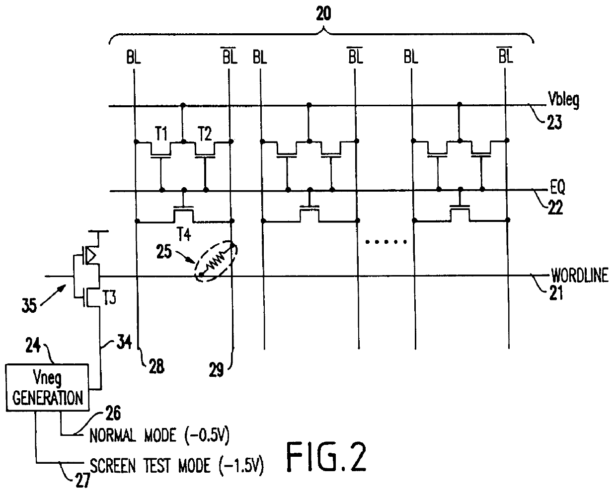
A first embodiment, shown in FIG. 2, is a DRAM device used with a conventional negative wordline protocol. FIG. 2 illustrates a schematic circuit diagram including bitlines 20, a wordline 21, an equalization control (EQ) line 22, an equalization supply (Vbleq) line 23, a negative voltage generator 24, a short 25 between one of the bitlines 20 and the wordline 21, a normal mode (e.g., -0.5V) input signal 26, an excessive voltage screen test mode (e.g., -1.5V) input signal 27 and precharge transistors T1, T2. As would be known by one ordinarily skilled in the art given this disclosure, the circuit illustrated in FIG. 2 selectively connects bitlines 10 to the equalization supply line 23 (using the transistors T1, T2) to equalize the voltage of the pairs of bitlines (e.g., complementary bitlines) 10 within the integrated circuit device.

In this embodiment, the negative wordline voltage supply 24 is designed so that during burn-in stress, the voltage level can be held at a level significa...

second embodiment

the invention, which is illustrated in FIGS. 4 and 5 comprises a DRAM structure for use with a conventional boosted wordline approach. The same features discussed above are given the same identification numbering in the drawings and a redundant discussion of the same is omitted for sake of brevity.

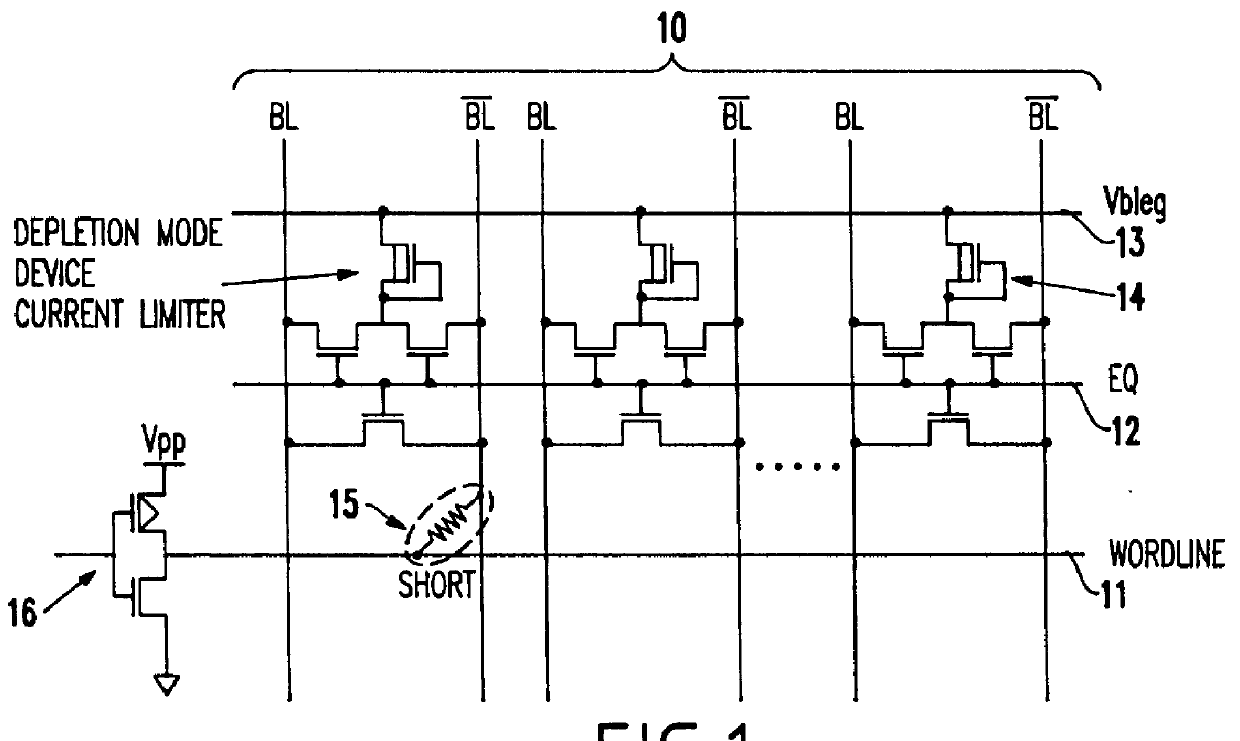
More specifically, during the screening test, the boosted wordline supply 41 (e.g., Vpp), is connected to the Vbleq line 23 in place of the normally connected Vbleq generator 40. At the same time, all the wordlines 21 are held at ground. The voltage on the defective bitlines 28, 29 approach zero, since they are discharged to ground through the "complete short" 25. When the EQ line 22 is turned on, the precharge devices (T1 and T2) of the defective bitlines 28, 29 are again subjected to hot carrier stress, as described above, which effectively disconnects the defective bitlines from the integrated circuit device.

The voltages within the device structures T1, T2 during burn-in stress are show...

third embodiment

FIG. 6 illustrates the invention useful with the substrate hot carrier programming approach. Once again, similar features are identified with similar numbers. In addition to the precharge devices T1 and T2, show in FIG. 6, multiplexer (MUM devices 61 connected to multiplexer control lines 62 are used to switch the array to a sense amplifier (not shown). With the invention, the MUX devices 61 can also be programmed so that the MUX 60 of defective bitline 29 acts as a current limiter.

More specifically, in this embodiment, during the screen test mode, the Vbleq line 23 is charged up to Vpp (e.g. 3.3V) and the wordline driver 35 is pulled low so that wordline 21 is at a negative voltage (e.g. -0.5V). Since bitline 29 is dead shorted to the wordline 21, bitline 29 is pulled low to the negative voltage. The drain of the MUX device 60, is at Vpp while its source is at Vneg, thus, the MUX device 60 will be programmed. In other words, the threshold voltage of the MUX 60 will be increased sig...


PUM


Abstract

A method and structure for disconnecting shorted bitlines from a dynamic random access memory circuit includes supplying a precharge voltage to equalization lines in the integrated circuit, supplying a negative voltage to wordlines in the integrated circuit, activating equalization devices connected to the bitlines and the equalization lines and maintaining the precharge voltage and the negative voltage until a short between one of the bitlines and one of the wordlines causes a corresponding equalization device of the equalization devices to have a permanently elevated threshold voltage.

Description

1. Field of the InventionThe present invention generally relates to integrated circuit memory arrays and more particularly to automatically removing shorted bitlines and wordlines from the memory arrays.2. Description of the Related ArtA "cross fail" is defined as a low resistance leakage path between two lines in an integrated circuit, such as a wordline and a bitline in a memory array. Undesirably large current may be drawn from the voltage supply to ground when a cross fail occurs. For example, in 64 M dynamic random access memory (DRAM) design, each cross fail could increase stand-by current by as much as 300 mA. In order to limit the current flow, a current limiter device such as a depletion mode-N type field effect transistor (NFET) device has conventionally been used.FIG. 1 illustrates a schematic circuit diagram including bitlines 10, a wordline 11, an equalization control (EQ) line 12, an equalization voltage supply (Vbleq) line 13, a current limiter (e.g., depletion mode d...

Claims


Application Information

Patent Timeline
IPC IPC(8): G11C11/403G11C29/02G11C29/50G11C29/04G11C11/404
CPCG11C11/404G11C29/50G11C29/025G11C29/02G11C11/401
Inventor HSU, LOUIS L. C.LA ROSA, GIUSEPPEMANDELMAN, JACK A.
Owner IBM CORP
Why Eureka
Try Eureka