Method of depositing a low k dielectric with organo silane

a dielectric and organo silane technology, applied in the field of semiconductor substrate fabrication, can solve the problems of new problems in the manufacturing process of integrated circuits, damage to device structures, and little or no improvement in the overall stack dielectric constant and capacitive coupling

Inactive Publication Date: 2000-04-25
APPLIED MATERIALS INC
View PDF73 Cites 671 Cited by
  • Summary
  • Abstract
  • Description
  • Claims
  • Application Information

AI Technical Summary

Problems solved by technology

The high temperatures at which some thermal CVD processes operate can damage device structures having layers previously formed thereon.
However, these materials present new problems for integrated circuit manufacturing processes.
Conventional liner layers, such as SiN, have higher dielectric constants, and the combination of low k dielectric layers with high k dielectric liner layers may result in little or no improvement in the overall stack dielectric constant and capacitive coupling.
The benefit of some low k dielectric materials is further compromised by low oxide content which makes the material inadequate as an etch stop layer.
This may lead to cross talk and / or resistance-capacitance (RC) delay which degrades the overall performance of the device.

Method used


Image

  • Method of depositing a low k dielectric with organo silane
  • Method of depositing a low k dielectric with organo silane
  • Method of depositing a low k dielectric with organo silane

Examples


example

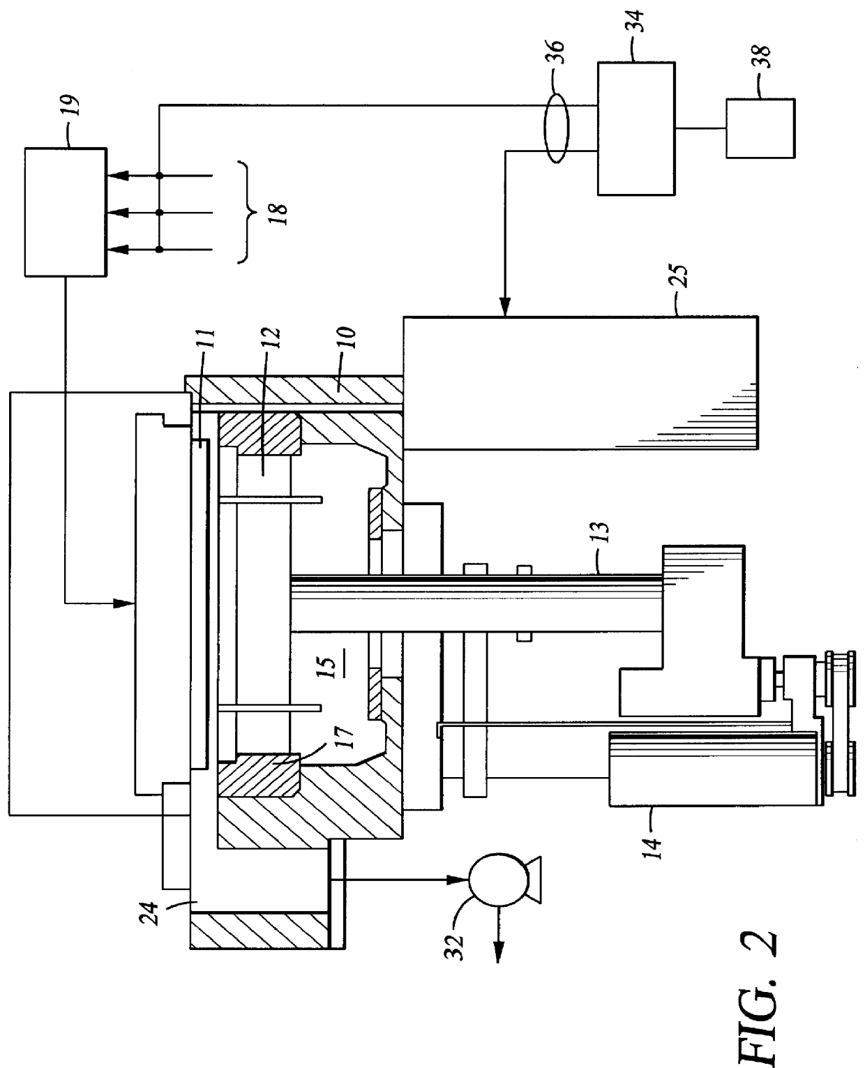
The following example demonstrates deposition of an oxidized organo silane film having excellent barrier and adhesion properties. This example was undertaken using a chemical vapor deposition chamber, and in particular, a "CENTURA DxZ" system which includes a solid-state RF matching unit with a two-piece quartz process kit, both fabricated and sold by Applied Materials, Inc., Santa Clara, Calif.

An oxidized methyl silane film was deposited at a chamber pressure of 3.0 Torr and temperature of 0.degree. C. from reactive gases which were flown into the reactor as follows:

The substrate was positioned 600 mil from the gas distribution showerhead and 80 W of high frequency power (13 MHz) was applied to the showerhead for plasma enhanced deposition of an oxidized methyl silane layer.

The oxidized methyl silane material was deposited at a rate of 1800 .ANG.. The deposited film had a dielectric constant of 3.0 and a refractive index of 1.44. The film had a measured tensile stress of 0.8.times....


PUM

PropertyMeasurementUnit
temperatureaaaaaaaaaa
frequencyaaaaaaaaaa
RF poweraaaaaaaaaa

Abstract

A method and apparatus for depositing a low dielectric constant film by reaction of an organo silane compound and an oxidizing gas. The oxidized organo silane film has excellent barrier properties for use as a liner or cap layer adjacent other dielectric layers. The oxidized organo silane film can also be used as an etch stop or an intermetal dielectric layer for fabricating dual damascene structures. The oxidized organo silane films also provide excellent adhesion between different dielectric layers. A preferred oxidized organo silane film is produced by reaction of methyl silane, CH3SiH3, and N2O.

Description

BACKGROUND OF THE DISCLOSURE1.Field of the InventionThe present invention relates to the fabrication of integrated circuits. More particularly, the invention relates to a process and apparatus for depositing dielectric layers on a semiconductor substrate.2. Background of the InventionOne of the primary steps in the fabrication of modem semiconductor devices is the formation of metal and dielectric films on a semiconductor substrate by chemical reaction of gases. Such deposition processes are referred to as chemical vapor deposition or CVD. Conventional thermal CVD processes supply reactive gases to the substrate surface where heat-induced chemical reactions take place to produce a desired film. The high temperatures at which some thermal CVD processes operate can damage device structures having layers previously formed thereon. A preferred method of depositing metal and dielectric films at relatively low temperatures is plasma-enhanced CVD (PECVD) techniques such as described in U.S...

Claims


Application Information

Patent Timeline
Patent Type & Authority Patents(United States)
IPC IPC(8): C23C16/40H01L21/02H01L21/768H01L21/70H01L21/316
CPCC23C16/401H01L21/76837H01L21/02164H01L21/02211H01L21/02274H01L21/02304H01L21/02362H01L21/3122H01L21/31612H01L21/31633H01L21/76801H01L21/7681H01L21/76828H01L21/76829H01L21/76832H01L21/76834H01L21/76835H01L21/02126
Inventor YAU, WAI-FANCHEUNG, DAVIDJENG, SHIN-PUULIU, KUOWEIYU, YUNG-CHENG
Owner APPLIED MATERIALS INC
Why Eureka
Try Eureka