Nonvolatile memory cell using microelectromechanical device

a non-volatile, memory cell technology, applied in microstructural devices, microstructured devices, relays, etc., can solve the problems of no storage means within the switch device, oxide stress degradation, and the need for extra high-voltage power supply of dual-polysilicon device designs

Inactive Publication Date: 2000-04-25
IBM CORP
View PDF11 Cites 116 Cited by
  • Summary
  • Abstract
  • Description
  • Claims
  • Application Information

AI Technical Summary

Benefits of technology

In another aspect, the present invention provides a nonvolatile memory cell comprising a first conductive element in a first charge state, a second conductive element in a second charge state and means for bringing the first and second conductive elements into electrical contact to effect a charge state change in one of the first and second conductive elements. The cell also includes means for sensing the charge state in the one of the first and second conductive elements. Preferably, the first conductive element comprises a cantilever beam and the second conductive element comprises a FET gate. The means for bringing the first and second conductive elements into electrical contact to effect a charge state change may comprise an electrode which applies an electrostatic attractive force to the first conductive element and the means for sensing the charge state may comprise a FET. Preferably, the memory cell is fabricated on an insulating layer that can be fabricated on a substrate such as a silicon wafer. A protective layer of silicon nitride may be provided over the insulating layer covering the first and second conductive elements.
In a further aspect, the present invention provides a nonvolatile memory cell comprising a conductive cantilever beam having a free end in a first charge state, a sensing element such as an FET having a conductive gate in a second charge state, the sensing element adapted to sense the charge state in the gate, and an electrode adapted to bring the cantilever beam into electrical contact with the gate to effect a charge state change in the gate. The cantilever beam is preferably electrically conductive polysilicon over its entire length and a polysilicon electrode is adapted to apply an electrostatic attractive force to the cantilever beam. The cell may further include a protective layer of silicon nitride over the insulating layer covering the cantilever beam, electrode and FET.
In a related aspect, the present invention provides a method of creating and sensing a charge state in a nonvolatile memory cell comprising providing a first conductive element in a first charge state and providing a second conductive element in a second charge state. The first and second conductive elements are electrically contacted to effect a charge state change in one of the first and second conductive elements. The charge state is sensed in the one of the first and second conductive elements.

Problems solved by technology

Dual polysilicon device designs can suffer from the need for extra high voltage power supplies and from gate oxide stress degradation.
However, the switch utilizes an insulated cantilever beam and provides no storage means within the switch device.

Method used


Image

  • Nonvolatile memory cell using microelectromechanical device
  • Nonvolatile memory cell using microelectromechanical device
  • Nonvolatile memory cell using microelectromechanical device

Examples


Embodiment Construction

)

In describing the preferred embodiment of the present invention, reference will be made herein to FIGS. 1-20 of the drawings in which like numerals refer to like features of the invention. Features of the invention are not necessarily shown to scale in the drawings.

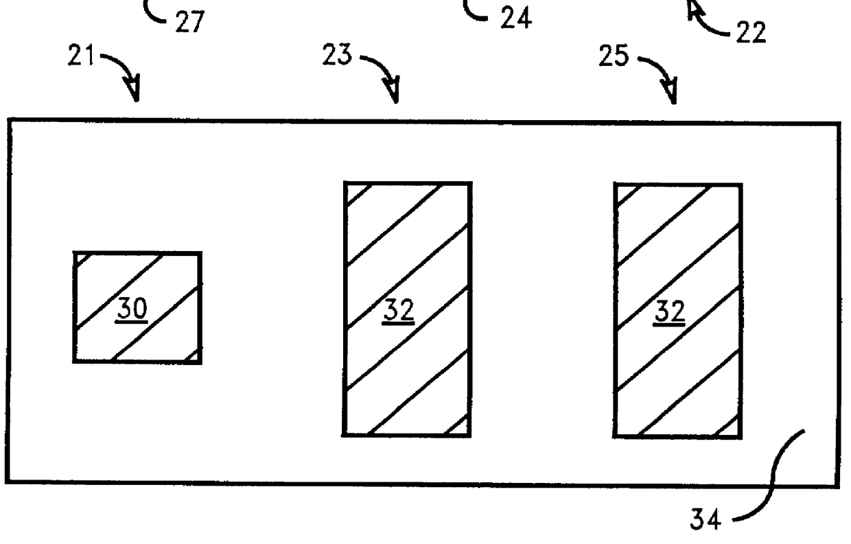
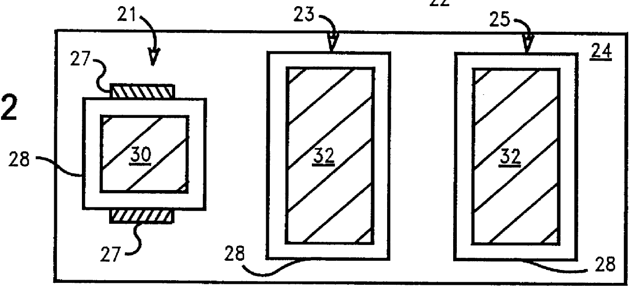
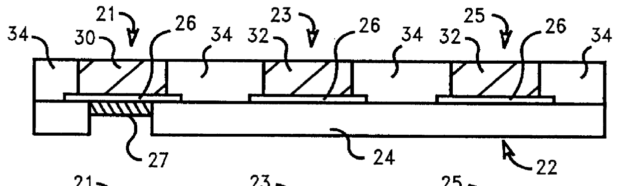
The present invention is directed to a nonvolatile memory cell structure which consists of a microelectromechanical switch which utilizes an electrostatic pull-in electrode to actuate the switch and an otherwise conventional MOSFET as a storage device. When the pull-in voltage is high enough, the switch arm is pulled closed, causing a charge to be deposited on the MOSFET gate. The gate is electrically isolated similar to the floating gate of a conventional NVRAM (nonvolatile random access memory) cell and is therefore nonvolatile. The amount of stored charge is electrically sensed by measuring the source-drain current through the MOSFET. The invention as described uses an n-channel FET although it could also be applied t...


PUM


Abstract

A nonvolatile memory cell comprises a conductive cantilever beam having a free end in a first charge state, a first FET having a conductive gate in a second charge state and a pull-in electrode adapted to bring the cantilever beam into electrical contact with the gate to effect a charge state change in the gate. A pull-in electrode input is connected to the electrode, a cantilever input is connected to the cantilever, a column select input is connected to the first FET and a row select input is connected to the first FET. The nonvolatile memory cell is selected by signals applied to the row select input and the column select input. The cell also includes a second FET connected between the cantilever beam and the cantilever input for controlling the passage of signals from the cantilever input to the cantilever beam and a third FET connected between the pull-in electrode and the pull-in electrode input for controlling the passage of signals from the pull-in electrode input to the electrode. The second FET and third FET have gates connected to the row select input. The row select input turns on the second FET and the third FET to allow the passage of signals from the pull-in electrode input to the pull-in electrode and from the cantilever input to the cantilever beam when the nonvolatile memory cell is selected.

Description

1. Field of the InventionThis invention relates generally to microelectromechanical devices used in electronic circuits and is directed in particular to a nonvolatile memory cell using an integrated microelectromechanical device made by a photolithographic process.2. Description of Related ArtConventional nonvolatile VLSI memory technologies use a dual polysilicon process consisting of a stacked control gate and a floating gate over a MOSFET (metal oxide semiconductor field effect transistor) channel. Under the proper voltage conditions, the floating gate becomes charged with carriers that have tunneled through the oxide from the MOSFET channel. This charge alters the device threshold enough to be electrically sensed. The level of the charge corresponds to either a 0 or 1 signal so that the device can be used as a memory cell in, for example, random access memory in a computer.Dual polysilicon device designs can suffer from the need for extra high voltage power supplies and from gat...

Claims


Application Information

Patent Timeline
Patent Type & Authority Patents(United States)
IPC IPC(8): B81B3/00H01L27/105H01H59/00
CPCH01L27/105H01H59/0009
Inventor NAKOS, JAMES S.WILLIAMS, RICHARD Q.
Owner IBM CORP
Why Eureka
Try Eureka