Method for forming isolation regions subsequent to gate formation and structure thereof

Inactive Publication Date: 2000-05-30
INTEGRATED DEVICE TECH INC
View PDF16 Cites 48 Cited by
  • Summary
  • Abstract
  • Description
  • Claims
  • Application Information

AI Technical Summary

Benefits of technology

In accordance with the present invention, improved semiconductor devices and methods of fabrication thereof are enabled. In embodiments of the present invention, a masking layer is formed and patterned to expose a first region of a semiconductor substrate. The first region is implanted with a first predetermined dose of oxygen ions, nitrogen ions or a combination thereof, at a predetermined energy level to create a predetermined concentration of the selected ion

Problems solved by technology

However, despite their broad application, LOCOS based processes all have several drawbacks.
The first of these drawbacks is the formation of a "Bird's Beak" region under a portion of the oxidation resistant layer or mask.
While variations of the basic LOCOS process, in particular Poly-Buffer LOCOS (PBL), have served to reduce the size of the "Bird's Beak" region, "Bird's Beak" formation can still restrict the usefulness of such LOCOS processes for deep sub-micron devices (below about 0.5 .mu.m (micron)).
Also, as thermal oxidation of silicon is the conversion of a volume of silicon to approximately two times that volume of silicon oxide, the resulting structure is non-planar.
Finally, the various LOCOS processes suffer from oxide thin

Method used


Image

  • Method for forming isolation regions subsequent to gate formation and structure thereof
  • Method for forming isolation regions subsequent to gate formation and structure thereof
  • Method for forming isolation regions subsequent to gate formation and structure thereof

Examples


Embodiment Construction

As embodiments of the present invention are described with reference to the aforementioned drawings, various modifications or adaptations of the specific structures and / or methods may become apparent to those skilled in the art. All such modifications, adaptations, or variations that rely upon the teachings of the present invention, and through which these teachings have advanced the art, are considered to be within the spirit and scope of the present invention.

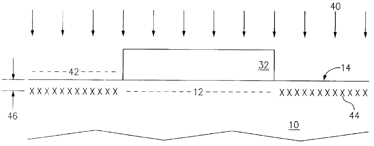
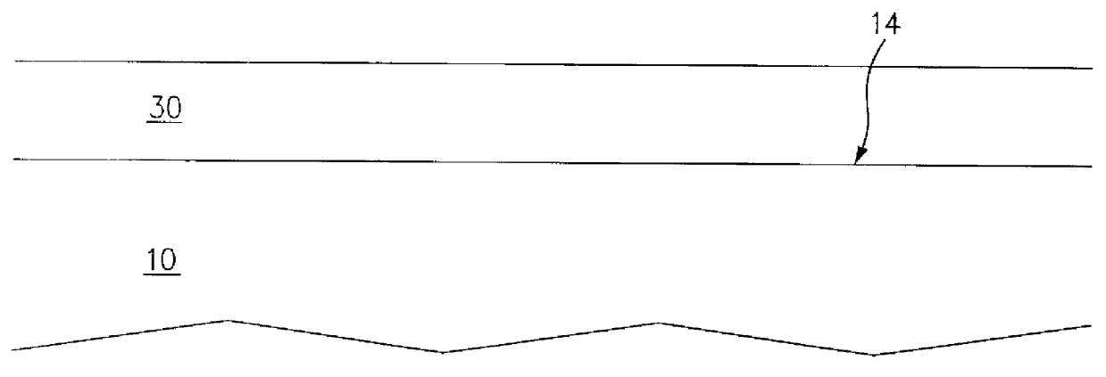
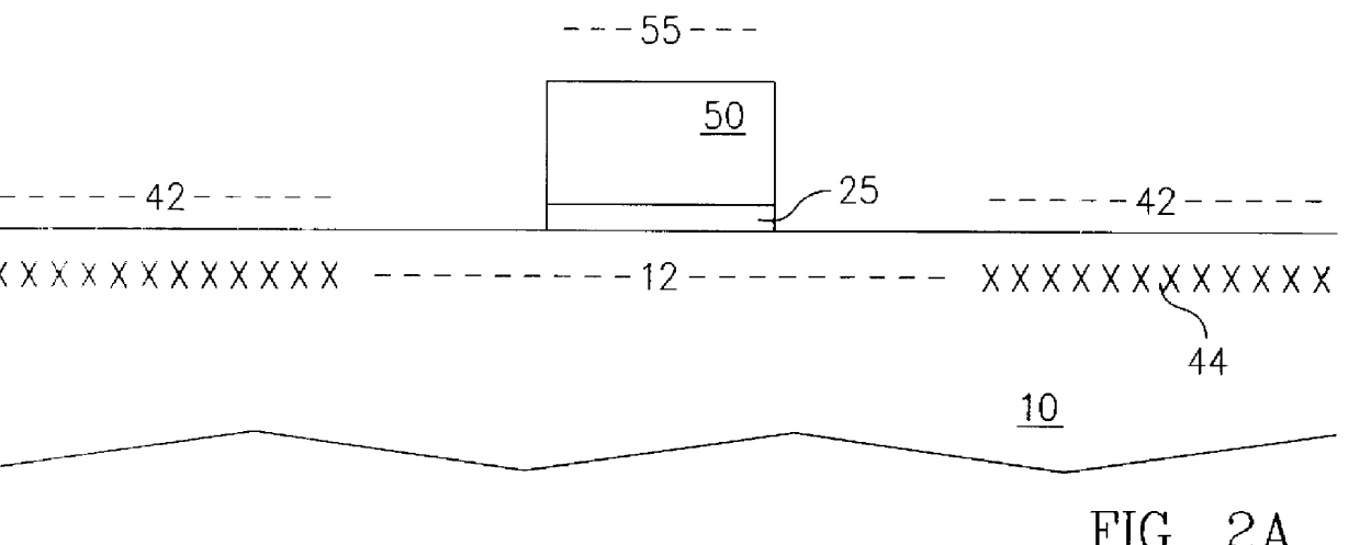
Referring to FIG. 1A, a semiconductor substrate at an early stage in the fabrication of a semiconductor device, e.g. a transistor, is depicted. A semiconductor substrate or wafer 10 is depicted having an implant masking layer 30 disposed on an upper surface 14. While wafer 10 is depicted in FIG. 1A as having a minimum of complexity, other types of substrates or wafers can be advantageously employed. For example, substrate 10 can be a single crystal N-type or P-type substrate, an N-type or P-type substrate encompassing an epit...


PUM


Abstract

Semiconductor devices are formed in a semiconductor substrate having an essentially planar upper surface. In some embodiments, implanted regions are formed in the substrate at a first predetermined depth by implantation of oxygen and/or nitrogen ions. In some embodiments buried implanted are formed in the substrate at a second predetermined depth, deeper than the first depth by implantation of oxygen and/or nitrogen ions. These implanted regions are converted to dielectric isolation regions and buried dielectric regions, respectively, by a high temperature anneal after formation of a gate structure.

Description

BACKGROUND1. Field of the InventionThis invention relates generally to a method for fabricating semiconductor devices and the devices so formed, and specifically to a method for forming isolation regions after formation of a gate electrode and the semiconductor devices so formed.2. Related ArtIn the manufacture of high performance Metal On Semiconductor (MOS) and combined Bipolar and MOS (BiMOS) semiconductor devices, each individual device structure is typically electrically isolated from other device structures through an isolation region. Formation of such isolation regions generally falls into two major categories. The first category encompasses all of the variations of LOCOS (LOCal Oxidation of Silicon) and involves exposing silicon to an oxidizing atmosphere to form silicon oxide. The second category includes the various trench forming and filling isolation structures, and thus requires etching a portion of the substrate and then refilling the etched portion with a dielectric ...

Claims


Application Information

Patent Timeline
IPC IPC(8): H01L21/762H01L21/70
CPCH01L21/76213
Inventor CHOI, JEONG Y.
Owner INTEGRATED DEVICE TECH INC
Why Eureka
Try Eureka