Eureka AIR delivers breakthrough ideas for toughest innovation challenges, trusted by R&D personnel around the world.

Random access memory having bit selectable mask for memory writes

Inactive Publication Date: 2000-06-13
GLOBALFOUNDRIES INC
View PDF8 Cites 11 Cited by
  • Summary
  • Abstract
  • Description
  • Claims
  • Application Information

AI Technical Summary

Benefits of technology

Another aspect of the present invention provides a random access memory circuit comprising an array of memory cells arranged in a first number of columns having a second number of rows, each column of memory cells addressed by a corresponding set of bit lines and each row of cells addressed by a corresponding word line, each memory cell including a logic gate for generating a gating signal in response to a supplied write signal and a bit enable signal, the gating signal causing the corresponding memory cell to overwrite a stored data value with a supplied data value, and control logic for supplying the bit enable signal to a selected group of said columns in response to a mask signal. The control logic provides maximum flexibility in the configuration of the array, enabling the random access memory circuit to be configured as a variable-width memory without the necessity of additional external decoding logic. Moreover, the control logic enables selected bits of an addressed word to be written to, without overwriting unselected bits in the addressed word. Hence, individual bits of an addressed word may be modified within a single clock cycle, without the necessity of performing a read-modify-write sequence of operations requiring at least three clock cycles plus external logic to manipulate the individual bits of the addressed word.
Still another aspect of the present invention provides a method of selectively writing a data value to a static random access memory (SRAM) cell having a bistable latch, comprising supplying the data value to the bistable latch, and selectively connecting the bistable latch to a voltage source to cause writing of the data value into the bistable latch in response to a write data signal and a bit enable signal. Selective connection of the bistable latch to the voltage source ensures that overwriting of data can be avoided, despite assertion of the appropriate address and write enable signals, by preventing connection of the bistable latch to a voltage source which would otherwise change the state of the bistable latch.

Problems solved by technology

Thus, this read-modify-write technique requires at least three clock cycles to modify a single bit in the memory configured for reading and writing on a per-byte basis, and requires additional external logic that increases the size and cost of the IC chip.

Method used


Image

  • Random access memory having bit selectable mask for memory writes
  • Random access memory having bit selectable mask for memory writes
  • Random access memory having bit selectable mask for memory writes

Examples


Embodiment Construction

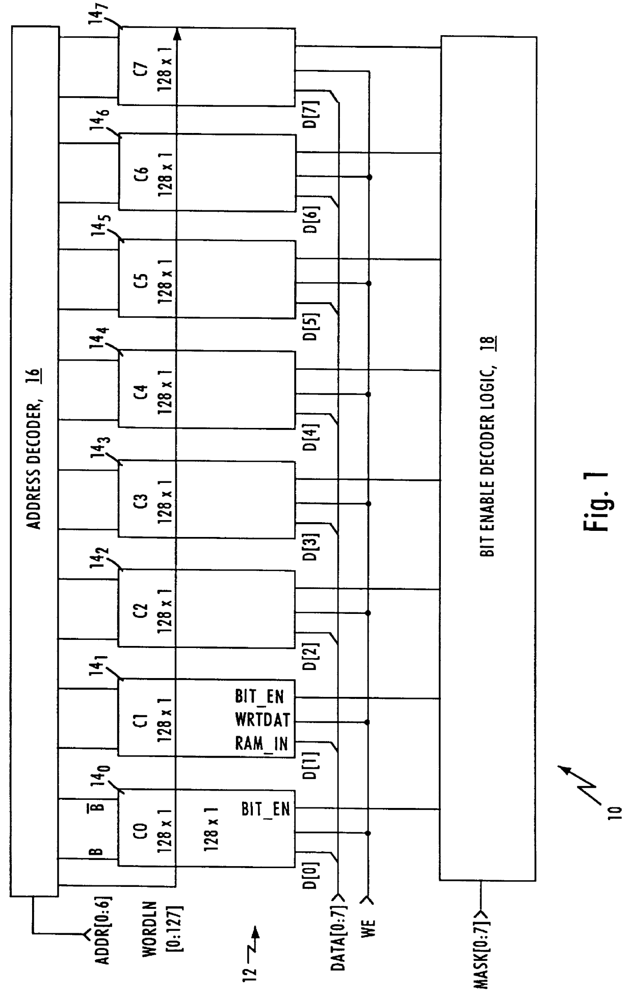
FIG. 1 is a block diagram illustrating a 128.times.8 RAM having a variable width configuration in accordance with an embodiment of the present invention. The RAM 10 is composed of an array of memory cells 12 arranged in eight columns 14 (C0-C7), where each column 14 is a 128 by 1-bit array of SRAM cells. The RAM 10 also includes an address decoder 16 and bit enable decoder logic 18, described below. The address decoder 16 is configured as a conventional 128 by 8-bit decoder, where the address decoder 16 asserts a selected one of the word lines (WORDLN[0:127]) in response to the 7-bit address signal (ADDR). The address decoder also asserts the bit line B, B# (i.e., "NOT B"=B#) on each of the columns 14. Hence, the RAM 10 may operate as a conventional memory, where each bit of the input data (DATA[0:7]) is written into a corresponding column array 14 at a selected row specified by a corresponding one of the word lines (WORDLN) and in response to the write enable signal (WE). According...


PUM


Abstract

A random access memory (RAM) having a prescribed number of bits defining a word length includes memory cells that enable selective overwriting on a bit-by-bit basis. Each memory cell includes a logic gate for generating a gating signal in response to a supplied write signal and a bit enable signal. The gating signal selectively connects the bistable latch of the memory cell to a voltage source to enable storage of the supplied data bit. Hence, selected bits can be written to an address word, without overwriting the unselected bits in the stored word, by supplying a mask signal that selectively drives the logic gates of the selected bits. The mask signal can also be used to configure a RAM as a dynamic-width memory, enabling use of the RAM for variable-width storage applications without the necessity of external decoding logic.

Description

1. Related ApplicationsThis application claims priority from provisional patent application Ser. No. 60 / 038,025, filed Feb. 14, 1997, entitled INTEGRATED MULTIPORT SWITCH (attorney docket 1033-230PRO), which is incorporated herein by reference.2. Technical FieldThe present invention relates to apparatus and methods for writing a selected bit of a word into a random access memory (RAM) having a prescribed number of bits defining a word length.3. Background ArtMemory architectures are typically configured to store a prescribed number of words having a predetermined word length. Such memory structures, known as word organized arrays, have a prescribed number of columns and rows, where the column length (i.e., the number of rows) equals the number of words, W, and the row length (i.e., the number of columns) equals the number of bits per word. Word selection is thus performed using a one-out-of-W decoder, i.e., a decoder with a mutually exclusive output for each word in the memory. The ...

Claims


Application Information

Patent Timeline
IPC IPC(8): G11C11/412H04L12/24H04L12/56H04Q3/545
CPCG11C11/412H04Q3/54591H04L41/0213
Inventor RUNALDUE, THOMAS JEFFERSONBOUN, SAMBUN
Owner GLOBALFOUNDRIES INC
Why Eureka
Eureka Blog
Learn More