Metal attachment method and structure for attaching substrates at low temperatures

a metal attachment and substrate technology, applied in the field of integrated circuits, can solve the problems of difficult to form fets with the channel other than parallel to the substrate, the size of transistors cannot generally be made smaller, and the miniaturization of fet devices has been limited

Inactive Publication Date: 2000-06-27
ADVANCED MICRO DEVICES INC
View PDF5 Cites 163 Cited by
  • Summary
  • Abstract
  • Description
  • Claims
  • Application Information

AI Technical Summary

Problems solved by technology

Several limitations on miniaturization of FET devices have been encountered.
For instance, it is extremely difficult to form FETs with the channel other than parallel to the substrate.
Thus, the size of the transistor cannot generally be made smaller than the size of the gate or the channel.
Furthermore, as the channel is made small, adverse effects on tr...

Method used


Image

  • Metal attachment method and structure for attaching substrates at low temperatures
  • Metal attachment method and structure for attaching substrates at low temperatures
  • Metal attachment method and structure for attaching substrates at low temperatures

Examples


Embodiment Construction

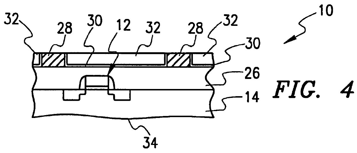
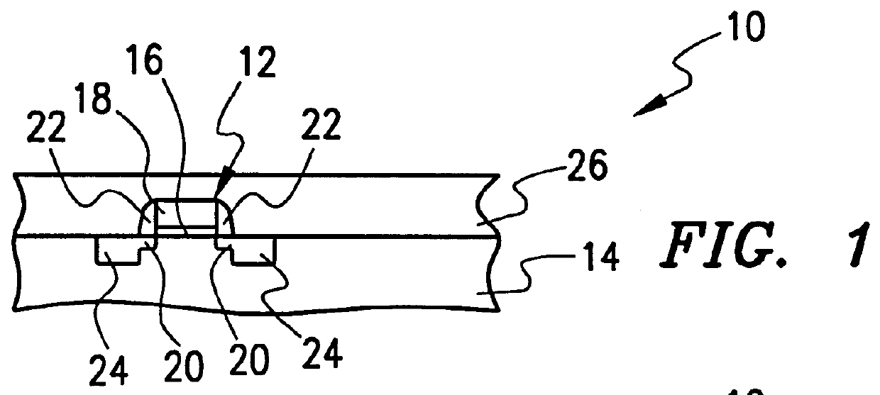
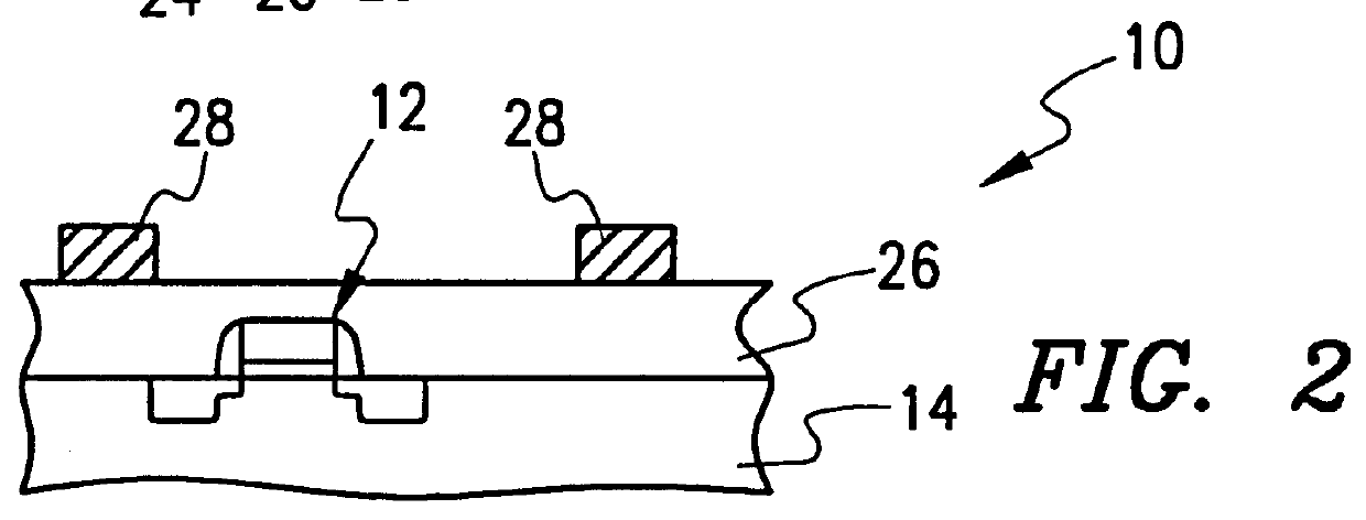
Turning now to FIGS. 1-4, the method of making a high density integrated circuit formed by low temperature fabrication of a first substrate structure having a transistor formation and metal interlevel lines thereon and a second substrate structure having a transistor formation and metal interlevel lines thereon shall be described with respect to the first substrate structure.

In FIG. 1, a first silicon substrate structure 10 includes desired transistor formations thereon, for example, such as high performance transistor formation 12. Structure further includes a substrate 14, preferably silicon, having a thickness on the order of 725 .mu.m.

The present invention provides for the fabrication of small geometry high performance MOS transistor devices. The range of geometries for high performance MOS transistor devices includes 0.1 to 0.2 microns, with respect to a minimum feature size, such as the high performance transistor gate length. The gate length always represents a minimum speed ...


PUM


Abstract

A high density integrated circuit structure and method of making the same includes providing a first silicon substrate structure having semiconductor device formations in accordance with a first circuit implementation and metal interlevel lines disposed on a top surface thereof and a second silicon substrate structure having a second circuit implementation and metal interlevel lines disposed on a top surface thereof. The first substrate structure includes a planarized low-K dielectric disposed between the metal interlevel lines and a protective coating separating the metal interlevel lines from is the low-K dielectric, the metal interlevel lines of the first silicon substrate structure have a melting temperature on the order of less than 500 DEG C. and the low-K dielectric having a dielectric K-value in the range of 2.0-3.8. The second substrate structure also includes a planarized low-K dielectric disposed between the metal interlevel lines and a protective coating separating the metal interlevel lines from the low-K dielectric, the metal interlevel lines having a melting temperature on the order of less than 500 DEG C. and the low-K dielectric having a dielectric K-value in the range of 2.0-3.8. Lastly, the first substrate structure is low temperature bonded to the second substrate structure at respective metal interlevel lines of the first and second substrate structures.

Description

1. Field of the InventionThis invention relates generally to integrated circuits and, more particularly, to a high density, high performance MOSFET structures and method of making the same.2. Discussion of the Related ArtA field-effect transistor (FET) is a solid state amplifying device. Amplification in the device occurs when the current through two terminals is varied by an electric field arising from voltage applied to a third terminal. The FET is thus a voltage controlled device. In an insulated-gate (IG) type of FET, the controlling field appears at an insulating layer. Variations in the field cause corresponding variations in the current through the device. Because the input or control voltage is applied across an insulator, the FET is further characterized by a high input impedance.In the IGFET, the channel current is controlled by a voltage at a gate electrode which is isolated from the channel by an insulator. In one common configuration, an oxide layer is grown or deposite...

Claims


Application Information

Patent Timeline
IPC IPC(8): H01L21/768H01L21/98H01L23/52H01L21/70H01L23/532H01L25/065
CPCH01L21/76801H01L21/76834H01L23/5329H01L25/0657H01L25/50H01L24/80H01L2924/1306H01L2924/13091H01L2224/80896H01L2224/80895H01L2224/05571H01L2225/06513H01L2225/06541H01L2924/3011H01L2224/80357H01L2924/00012H01L2924/00H01L2924/14H01L2224/05547H01L2224/80986H01L2224/8034H01L2224/80359H01L2224/0384
Inventor GARDNER, MARK I.HAUSE, FREDKADOSH, DANIEL
Owner ADVANCED MICRO DEVICES INC
Why Eureka
Try Eureka