Dielectric material with low temperature coefficient and high quality

a dielectric material and low temperature coefficient technology, applied in the field of multilayer circuit boards, can solve the problems of difficult to obtain homogeneous dielectric materials, inability to achieve the expected effect of correcting .tau..sub.f, and undesirable substrate materials of prior art for use in resonators or filters

Inactive Publication Date: 2000-09-19
NGK SPARK PLUG CO LTD
View PDF25 Cites 12 Cited by
  • Summary
  • Abstract
  • Description
  • Claims
  • Application Information

AI Technical Summary

Problems solved by technology

These prior art substrate materials are therefore undesirable for use in resonators or filters.
However, these inorganic fillers tend to react with glass ingredients or dielectric materials that include glass ingredients and Al.sub.2 O.sub.3 added thereto during the sintering process.
Use of those inorganic fillers also has another problem in that they react with a glass frit to form a solid solution, thus forming a disordered crystal structure, and making it impossible to obtain the expected effect of correcting .tau..sub.f.
If those inorganic fillers are added in large amounts, or if those inorganic fillers having a large particle diameter are added, two problems occur: (i) a homogeneous dielectric material is difficult to obtain, and (ii) a sufficiently densified sinter is difficult to obtain through low-temperature sintering.
No effective means have been proposed for improving the Q.sub.u of a dielectric material produced through low-temperature sintering.

Method used


Image

  • Dielectric material with low temperature coefficient and high quality
  • Dielectric material with low temperature coefficient and high quality
  • Dielectric material with low temperature coefficient and high quality

Examples


experimental examples 15 to 18

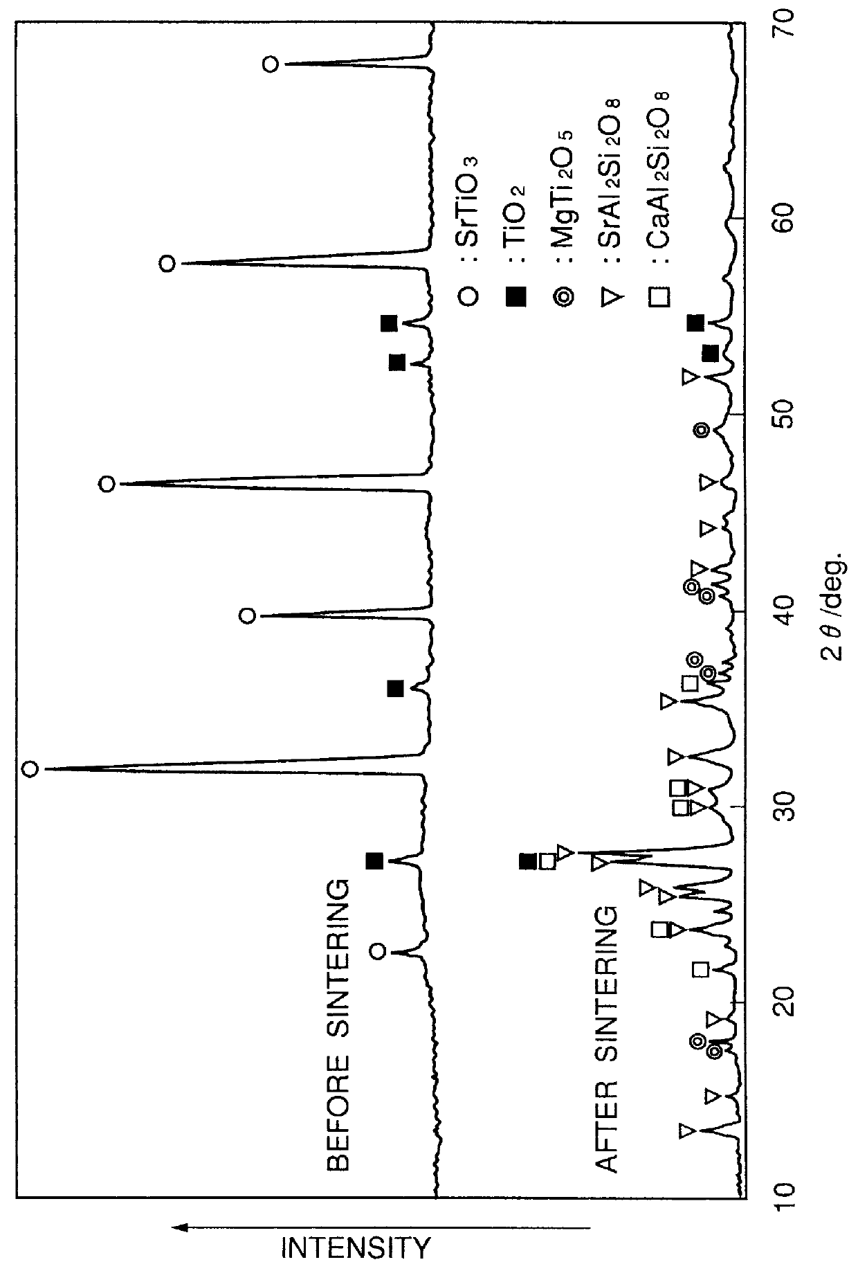
Using the same starting ingredients in the same proportion as in Experimental Example 2, dielectric materials were produced under the same conditions as in Experimental Example 2, except that sintering was conducted at the temperatures shown in Table 2. The dielectric materials thus obtained were evaluated for dielectric properties and examined for the component constituting the main crystalline phase, in the same manner as in Experimental Example 2. The results obtained are shown in

As noted, the dielectric material obtained in Experimental Example 18 had an exceedingly high dielectric loss and gave no resonance waveform; therefore, the dielectric properties of this Experimental Example could not be determined, as stated in Table 2.

The results given in Table 2 show the following. The dielectric materials obtained in Experimental Examples 15 and 16, respectively using sintering temperatures of 900.degree. C. and 950.degree. C., each had a water absorption lower than 0.1%, and had .ta...

experimental example 19

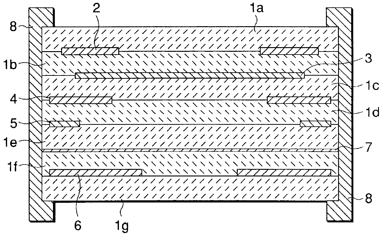
A glass ingredient prepared using the same starting ingredients in the same proportion as in Experimental Example 2 shown in Table 1 was mixed with the same powdery Sr compound and additive as in Experimental Example 2. These ingredients were mixed in ethanol and dried in the same manner as in Experimental Example 2. To this powder mixture were added an acrylic binder (ethyl methacrylate), a plasticizer (dioctyl phthalate), and a dispersant (a polymer partly esterified with maleic acid). These ingredients were sufficiently mixed in a toluene / methyl ethyl ketone mixed solvent to prepare a slurry. Subsequently, green tapes having predetermined thicknesses ranging between 0.1 and 1.2 mm were formed from the slurry by doctor blade method.

Using a silver paste for use in the formation of thick circuit films, conductor wiring patterns (thickness: 20-25 .mu.m) were formed by printing on the green tapes having various thicknesses in the above range, in order to form various electrodes such a...

first embodiment

In the present invention, there is provided a glass ceramic dielectric material, where the glass ceramic has strontium anorthite as a main crystalline phase.

In the second embodiment of the present invention, there is provided a dielectric material as described above in the first embodiment, such that the dielectric material may have TiO.sub.2 as another crystalline phase.

It is noted with respect to the first and second embodiments that the dielectric materials have a small absolute value of .tau..sub.f, a large value of Q.sub.u .times.f.sub.0, and a high density. Since these dielectric materials can be produced though low-temperature sintering, wiring patterns comprising a conductor, e.g., gold or silver, printed on green tapes from which the dielectric materials are to be obtained, can be sintered simultaneously with the green tapes.


PUM

PropertyMeasurementUnit
particle diameteraaaaaaaaaa
water absorptionaaaaaaaaaa
temperatureaaaaaaaaaa

Abstract

A dielectric material is disclosed which has a small absolute value of the temperature coefficient of resonance frequency and a high coefficient of unloaded quality. Also disclosed are a process for producing the dielectric material and multilayer and other circuit boards containing the dielectric material. The dielectric material is a highly densified material having a water absorption lower than 0.1%, which is obtained by mixing 95.5 to 99.5 percent by weight mixture of a glass frit and a strontium compound with 0.5 to 4.5 percent by weight titanium dioxide, compacting the resultant mixture, and sintering the compact at a relatively low temperature around 930 DEG C. This dielectric material is a glass ceramic containing strontium anorthite (SrAl2Si2O8) as the main crystalline phase, and may contain the TiO2, which remains unchanged after sintering. The absolute value of the temperature coefficient of resonance frequency of the dielectric material is 20 ppm/ DEG C. or lower, preferably 10 ppm/ DEG C. or lower, more preferably 5 ppm/ DEG C. or lower. The product of the unloaded quality coefficient and resonance frequency is 1,800 GHz or larger, preferably 2,500 GHz or larger. This material therefore has excellent dielectric properties.

Description

This application claims the benefit of Application No. Hei.8-277618, filed in Japan on Sep. 26, 1996, and Application No. Hei. 9-184567, filed in Japan on Jun. 24, 1997, both of which are incorporated by reference.The present invention relates to a field of dielectric materials having excellent dielectric properties in the microwave range. The present invention also relates to a process for producing the dielectric material. The present invention further relates to single and multi-layer circuit boards, which are obtained by forming a wiring pattern made of a conductive material, either on a surface of a substrate consisting of the dielectric material or between stacked substrates consisting of the dielectric material. The invention also relates to other devices used in such applications such as dielectric resonators and filters, particularly those operating in the microwave range.DISCUSSION OF RELATED ARTMultilayer circuit boards presently are obtained by sintering insulator layers...

Claims


Application Information

Patent Timeline
Patent Type & Authority Patents(United States)
IPC IPC(8): C03C10/00H01P7/08H05K1/03C04B35/18C03C10/06C04B35/00H01B3/02H01B3/12H05K3/46
CPCC03C10/0045H01P7/082H01P7/084H05K1/0306
Inventor YOKOI, HITOSHIMIZUTANI, HIDETOSHISATO, MOTOHIKOOHBAYASHI, KAZUSHIGE
Owner NGK SPARK PLUG CO LTD
Why Eureka
Try Eureka