

Method of manufacture of multilayer circuit boards
- Summary
- Abstract
- Description
- Claims
- Application Information
AI Technical Summary
Benefits of technology
Problems solved by technology
Method used
Image

Examples
Embodiment Construction
are also illustrative of the invention:
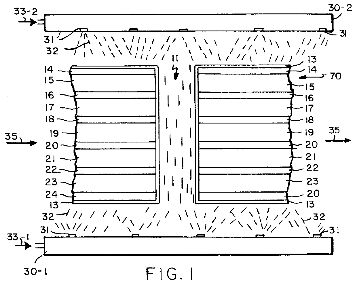
The copper clad parts (e.g., circuit board as shown in FIG. 1 with 30 holes as described below) were dipped in the above solvents in examples 1 to 21 for one minute at room temperature.
The parts were then rinsed with deionized water for one minute, then dried at 90.degree. C. for 5 minutes. The solvents were screened for performance by rating copper coverage in the 30 holes 14 mil diameter hole of a 0.094 inch thick circuit board. The coverage factor (CF) using se (as a control) in the same test was 2.2.
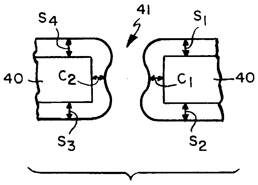
The coverage factor (CF) is determined as follows: A copper clad circuit board with thirty (30) holes, each through hole being 14 mil in diameter with the circuit board in which re formed being 0.094 inches in thickness. The circuit board 40 with the thirty holes 41 and with the conductive polypyrrole polymer coating 10 g / l as pyrrol with ethylbenzene sulfonate as the dopant and Rhodasurf TB 970 as the stabilizer to which there is applied the so...
PUM
| Property | Measurement | Unit |
|---|---|---|
| Electrical conductivity | aaaaa | aaaaa |
| Electrical conductor | aaaaa | aaaaa |
Abstract
Description
Claims
Application Information