Method of forming gate oxide having dual thickness by oxidation process

a technology of oxidation process and gate oxide, which is applied in the field of metal oxidesemiconductor (mos) field-effect transistors, can solve the problems of inability to provide effective, commercially practical method, and inability to use silicon nitride layers for gate oxides

Inactive Publication Date: 2000-09-26
INTEL CORP
View PDF15 Cites 86 Cited by
  • Summary
  • Abstract
  • Description
  • Claims
  • Application Information

AI Technical Summary

Problems solved by technology

The problem in realizing such an integrated circuit is that it requires for efficient operation, two different gate oxide thickness'.
No effective, commercially practical method has been found for providing these two different thickness' of oxides on the same substrate.
While it is known that silicon nitride may be used to inhibit the growth of an oxide layer thus, for instance, permitting field oxides of different thickness' to be produced such as shown in U.S. Pat. No. 4,352,236, the silicon nitride layers have not been suitable for use with gate oxides.

Method used


Image

  • Method of forming gate oxide having dual thickness by oxidation process
  • Method of forming gate oxide having dual thickness by oxidation process
  • Method of forming gate oxide having dual thickness by oxidation process

Examples


Embodiment Construction

A method for forming two different thicknesses of gate oxides is disclosed. In the following description numerous specific details are set forth, such as specific flow rates and thickness' in order to provide a thorough understanding of the present invention. It will be appreciated that the present invention may be practiced without these specific details. In other instances well-known steps, such as cleaning steps, are not described in detail in order not to obscure the present invention.

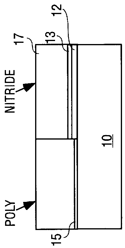
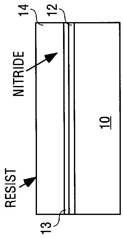
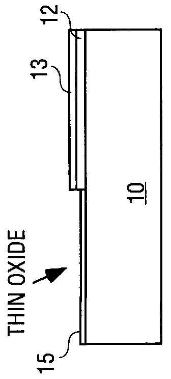
Referring now to FIG. 1, the monocrystaline silicon substrate 10 is first cleaned in a well-known manner using, for instance, a sacrificial oxide layer (e.g., silicon dioxide layer) and for instance, hydrofluoric acid. Then a first gate oxide 12 is formed on the substrate. This oxide may be formed with any one of a number of well-known steps and in one embodiment is thermally grown to a thickness of approximately 32 .ANG..

Next a silicon nitride layer 13 is formed on the oxide layer 12. This silicon...


PUM

PropertyMeasurementUnit
temperatureaaaaaaaaaa
thicknessaaaaaaaaaa

Abstract

Transistors are formed on the substrate having two different thickness' of gate oxides. A silicon nitride mask is used to protect one of the gate oxides while the other is grown. A nitride mask is formed from a hydrogen balanced nitride layer formed using direct plasma deposited nitride with an ammonia and silane chemistry. In one embodiment the nitride mask remains in place in the completed transistor.

Description

1. Field of the InventionThe invention relates to the field of metal-oxide-semiconductor (MOS) field-effect transistors (FETs) and more particularly, to the gate oxide used in these transistors.2. Prior ArtWhile the need for an integrated circuit which operates at two different power supply potentials has been recognized, its practical realization has been another matter. Such an integrated circuit would be useful to drive a bus at one potential while internally operating at another potential. This would permit, for instance, a new microprocessor to operate at a higher potential with older peripherals than the potential used internally for high speed logic circuits. There are numerous other applications where an integrated circuit operating at two potentials would be useful.The problem in realizing such an integrated circuit is that it requires for efficient operation, two different gate oxide thickness'. No effective, commercially practical method has been found for providing these...

Claims


Application Information

Patent Timeline
Patent Type & Authority Patents(United States)
IPC IPC(8): H01L21/70H01L21/8234
CPCH01L21/823462Y10S438/981
Inventor ARGHAVANI, REZABEATTIE, BRUCECHAU, ROBERT S.KAVALIEROS, JACKMCFADDEN, BOB
Owner INTEL CORP
Why Eureka
Try Eureka