Cleaner for inspecting projections, and inspection apparatus and method for integrated circuits

Inactive Publication Date: 2000-10-10
TOKYO ELECTRON LTD
View PDF6 Cites 69 Cited by
  • Summary
  • Abstract
  • Description
  • Claims
  • Application Information

AI Technical Summary

Benefits of technology

a cleaner layer fixed on the substrate, the cleaner layer having an elastic material layer and a material having a surface state improving function for the inspecting projections

Problems solved by technology

As the feature sizes of chips continue to decrease, the influence of contamination becomes prominent.
This burr removal is a complex operation.
In the membrane probe card, no means for effectively a

Method used


Image

  • Cleaner for inspecting projections, and inspection apparatus and method for integrated circuits
  • Cleaner for inspecting projections, and inspection apparatus and method for integrated circuits
  • Cleaner for inspecting projections, and inspection apparatus and method for integrated circuits

Examples


Embodiment Construction

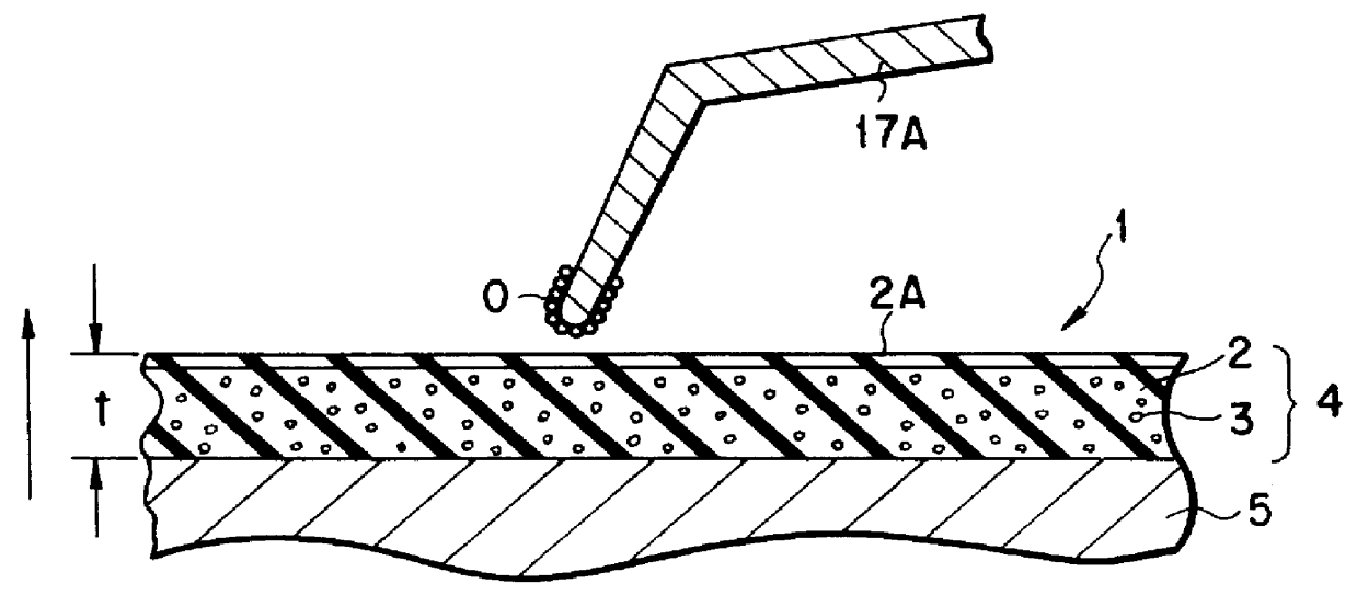
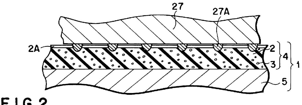
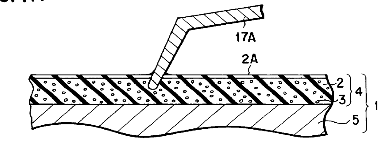
One embodiment of the present invention will be described with reference to FIGS. 1A, 1B and 2. A cleaner 1 according to this embodiment has a cleaner layer 4 and a substrate 5 on which the cleaner layer 4 is placed. The cleaner layer 4 is constituted by an elastic material layer 2 made of an elastic material (rubber), and a surface state improving filler (powdery material) 3 dispersed in the elastic material layer 2. As an application where the cleaner 1 is used, a case will be described wherein the cleaner 1 is used to clean probe needles 17A of a probe unit which inspects IC chips formed on a semiconductor wafer.

As the elastic material of the elastic material layer 2, either inorganic rubber or organic rubber can be used. In particular, inorganic rubber such as silicone rubber can be preferably used. As the filler 3, a material having a function of improving the surface state of the probe needles is selected. An example of the function that improves the surface state of the probe...


PUM


Abstract

A cleaner of this invention is a cleaner for inspecting projections and removes any substance, e.g., aluminum oxide, which attaches to needle points of probe needles, when the probe needles pierce into the cleaner. The cleaner has a cleaner layer and a substrate. The cleaner layer is constituted by an elastic material layer, and a filler having a surface state improving function of the inspecting projections and dispersed in the elastic material layer. As the filler having a surface state improving function, a powder including at least one of ceramic materials, e.g., sand, glass, alumina, Carborundum (trade name), and the like, or a fiber layer made of an inorganic fiber or organic fiber can be employed.

Description

BACKGROUND OF THE INVENTIONThe present invention relates to a cleaner for inspecting projections, and an inspection apparatus and method for integrated circuits having this cleaner.More particularly, the cleaner according to the present invention is a cleaner for inspecting projections (e.g., wire conductors such as probe needle or projecting conductors such as bump terminals) used for inspecting the electrical characteristics of integrated circuits and various types of mounted electronic components formed on a semiconductor wafer. The inspection apparatus and method for the integrated circuits according to the present invention are an inspecting apparatus and method having this cleaner, which inspect the electrical characteristics of integrated circuits formed on a semiconductor wafer.A prober is used as an inspection apparatus for inspecting the electrical characteristics of mounted electronic components, e.g., integrated circuits formed on a semiconductor wafer (to be referred to...

Claims


Application Information

Patent Timeline
IPC IPC(8): G01R31/316G01R31/28
CPCG01R31/316H01L22/00
Inventor YAMASAKA, RIKIHITO
Owner TOKYO ELECTRON LTD
Why Eureka
Try Eureka