Wiring board for electrical tests with bumps having polymeric coating

a technology of polymeric coating and wiring board, which is applied in the direction of printed circuit parts, printed element electric connection formation, instruments, etc., can solve the problems of difficult testing of devices and packaging circuit boards thereof, extremely difficult testing of such devices, and difficult to test so-called "bare chips"

Inactive Publication Date: 2000-10-17
HITACHI CHEM CO LTD
View PDF35 Cites 54 Cited by
  • Summary
  • Abstract
  • Description
  • Claims
  • Application Information

AI Technical Summary

Problems solved by technology

As semiconductor devices have been subjected to increased density of integration and density of surface packaging, the tests of the devices and the packaging circuit boards thereof have become very difficult.
The tests of such devices are extremely difficult.
Especially, it is difficult to test a so-called "bare chip" which is a silicon chip before being packaged (namely, before being mounted on a lead frame and encapsulated with a resin).
Granted that although testing of the bare chips is possible, it is not commonly undertaken because of complicated test jigs and heavy test expenses.
Such wiring circuit boards cannot be tested with regard to insulation and connection by a conventional method which permits the electrodes to be temporarily connected and disconnected.
When the copper foil is thicker, the amount of side etching or lateral etching enlarges in etching the copper foil in order to form the bump electrodes, making it impossible to form the high-density and high-accuracy bump electrodes.

Method used


Image

  • Wiring board for electrical tests with bumps having polymeric coating
  • Wiring board for electrical tests with bumps having polymeric coating
  • Wiring board for electrical tests with bumps having polymeric coating

Examples


Embodiment Construction

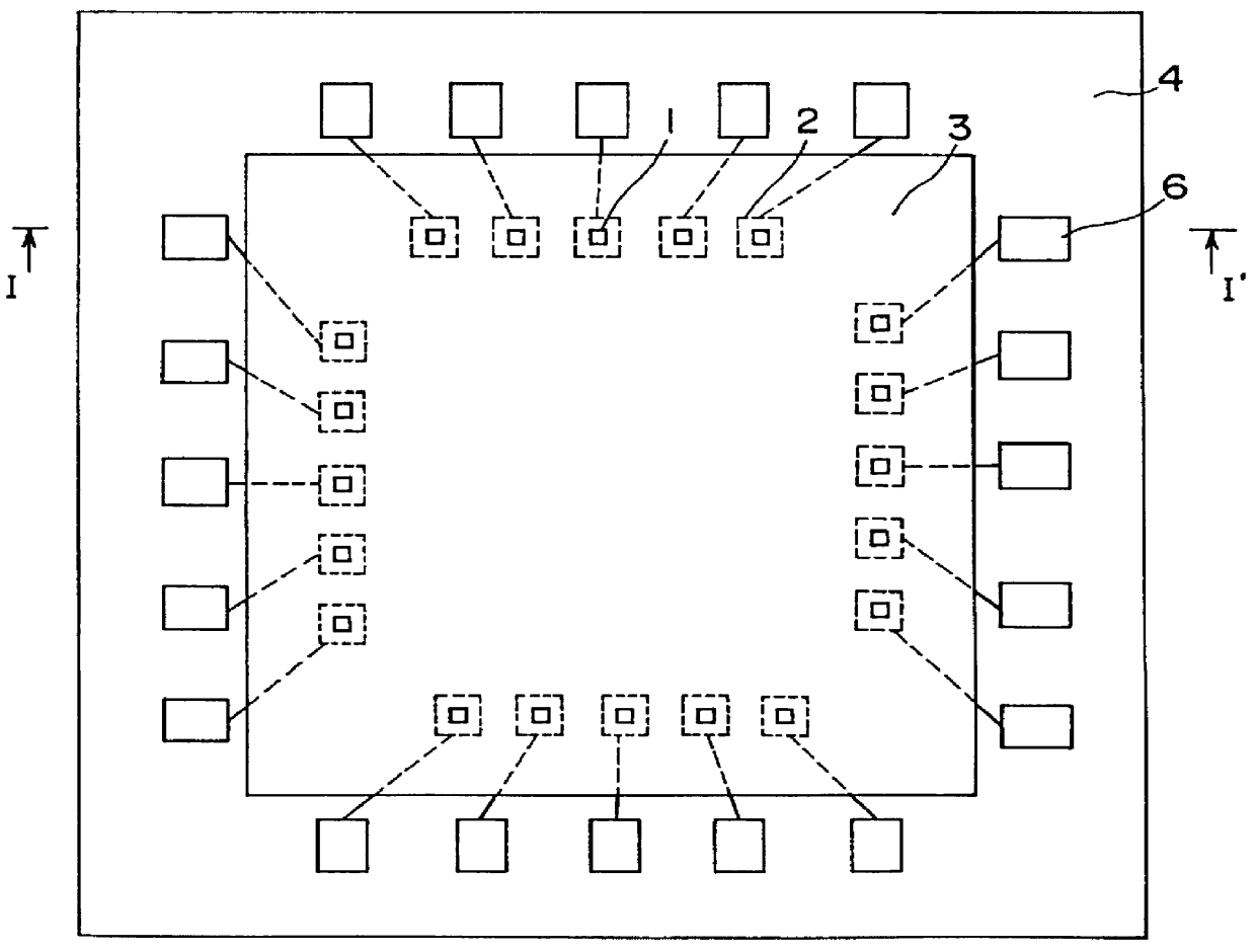
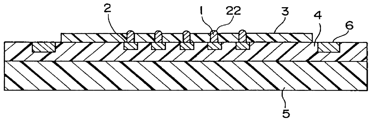
FIG. 1 is a sectional view showing a wiring board for electrical tests in an embodiment of the present invention, while FIG. 2 is a plan view showing the wiring board for electrical tests. The sectional view of FIG. 1 is taken along line I-I' and viewed in the direction of arrows as indicated in FIG. 2.

Referring to FIGS. 1 and 2, the wiring board in this embodiment comprises bump electrodes 1 which are respectively brought into contact with the corresponding electrodes of an article to-be-tested such as a semiconductor device, and wiring of predetermined pattern 2 which serves as lead-out lines for the bump electrodes 1. It also comprises a surface passivation layer 3, a resin layer 4, and a transparent substrate 5 which serves as an insulating substrate "transparent" means transparent to visible light. Further, external connection terminals 6 are formed in order to connect the lead-out lines 2 with measuring instruments which are arranged outside the wiring board. Incidentally, the...


PUM


Abstract

A wiring board for electrical tests; having an insulating substrate, wiring of predetermined pattern which is embedded in the insulating substrate, and bump electrodes which are formed on the wiring and which are respectively brought into contact with corresponding electrodes of an article to-be-tested. Thus, even when the electrode pitch of the article to-be-tested such as a semiconductor device has become smaller(for example, less than 0.1 [mm]), the electrodes can be formed so as to cope with the electrical tests of the article.

Description

1. Field of the InventionThe present invention relates to a wiring board for electrical tests. By way of example, the electrical tests include the insulation and connection tests of high-density wiring in a printed-wiring circuit board, a circuit board for an integrated circuit or a circuit board for a liquid-crystal display, and the ON-resistance tests of a semiconductor device.2. Description of the Related ArtAs semiconductor devices have been subjected to increased density of integration and density of surface packaging, the tests of the devices and the packaging circuit boards thereof have become very difficult.In the case of the semiconductor devices, several tens .about. several hundred of electrodes are laid out on silicon chips of several millimeters square. Further, a semiconductor device having more than one thousand electrodes will be developed. The tests of such devices are extremely difficult. Especially, it is difficult to test a so-called "bare chip" which is a silico...

Claims


Application Information

Patent Timeline
Patent Type & Authority Patents(United States)
IPC IPC(8): G01R1/073H05K3/20H05K3/40H05K3/46H05K3/04H05K3/06H05K3/02
CPCG01R1/07314H05K3/205H05K3/4007H05K3/4647H05K3/4658Y10S439/931H05K3/062H05K3/20H05K3/4652H05K2201/0355H05K2201/0361H05K2201/0367H05K2201/09509H05K2201/09563H05K2201/09781H05K2203/0152H05K2203/025H05K2203/0369H05K2203/0376H05K2203/0384H05K2203/0726H05K2203/0733H05K2203/1476H05K3/04
Inventor FUKUTOMI, NAOKINAKAMURA, HIDEHIRONAKAYAMA, HAJIMETSUBOMATSU, YOSHIAKINAKAMURA, MASANORIKAITOU, KOUICHIKUWANO, ATSUSHIWATANABE, ITSUOITABASHI, MASAHIKO
Owner HITACHI CHEM CO LTD
Why Eureka
Try Eureka