

Method for heat treatment of silicon substrate, substrate treated by the method, and epitaxial wafer utilizing the substrate
a technology of epitaxial wafers and silicon substrates, applied in the direction of after-treatment details, crystal growth process, polycrystalline material growth, etc., can solve the problems of poor accuracy, complex production operation, and degradation of device yield
Inactive Publication Date: 2000-11-07
SHIN-ETSU HANDOTAI CO LTD
View PDF3 Cites 35 Cited by
- Summary
- Abstract
- Description
- Claims
- Application Information
AI Technical Summary
Problems solved by technology
When the oxide precipitates are in the device active regions, they may be a cause of degradation of device yield.
Therefore, the production operation becomes complicated, and in addition the accuracy is bad.
Further, even though a crystal have a constant oxygen concentration along the crystal growth direction, the oxygen precipitation characteristic along the growth axis direction is not necessarily uniform due to influence of the thermal history during the crystal production.
To obtain uniform oxygen precipitation characteristic, heat treatment of long period of time is required, and hence the productivity becomes low.
On the other hand, as for an epitaxial wafer manufactured by using a silicon substrate produced by the CZ method, when epitaxial growth is performed using a silicon substrate having a usual resistivity, potential oxygen precipitation nuclei formed during the substrate production (crystal production) are eliminated by t
Method used
View moreImage
Smart ImageViewing Examples

Examples
 PUM
 Abstract
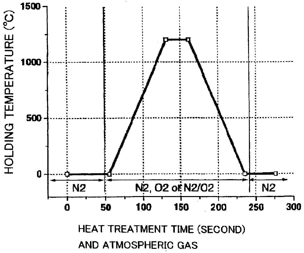
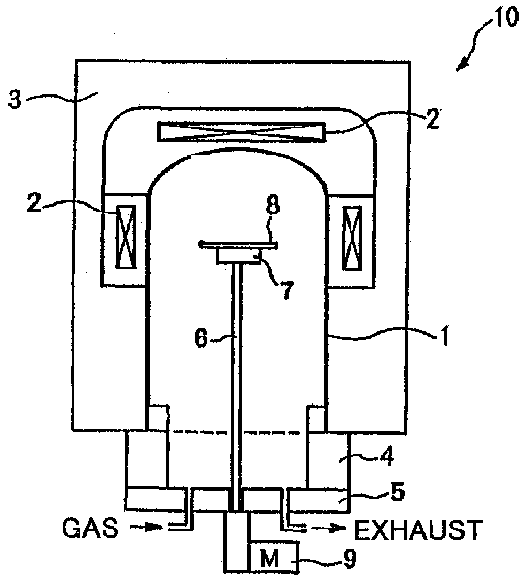
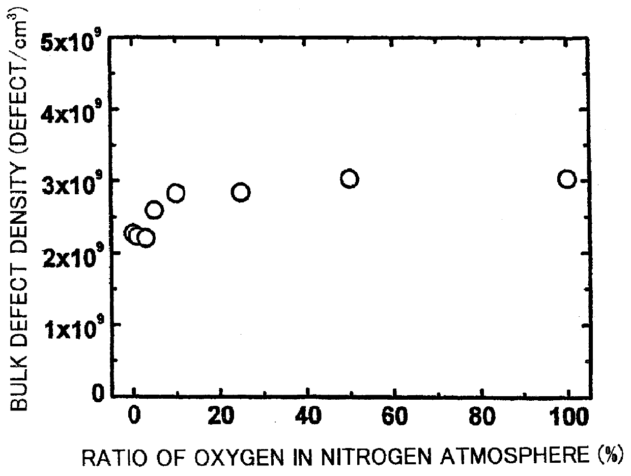
There is disclosed a method for heat treatment of a silicon substrate produced by the CZ method by utilizing a rapid thermal annealer, wherein the heat treatment is performed under an atmosphere composed of 100% nitrogen, or 100% oxygen, or a mixed atmosphere of oxygen and nitrogen by heating the silicon substrate to a maximum holding temperature within a range of from 1125 DEG C. to the melting point of silicon, and holding the substrate at that maximum holding temperature for a holding time of 5 seconds or more, and then the substrate is rapidly cooled at a cooling rate of 8 DEG C./second or more from the maximum holding temperature. In the method, the amount of oxygen precipitation nuclei in the substrate can be controlled by changing the maximum holding temperature and the holding time. The present invention provide a method for heat treatment of a silicon substrate produced by the CZ method by utilizing an RTA apparatus, which can provide a silicon substrate having a desired oxygen precipitation characteristic without controlling oxygen concentration in the silicon substrate, and an epitaxial wafer utilizing a substrate heat-treated by the method.
Description
1. Field of the InventionThe present invention relates to a method for heat treatment of a silicon substrate produced by the Czochralski method (CZ method), and an epitaxial wafer produced by using a substrate heat-treated by the method. In particular, it relates to a method for heat treatment for obtaining a semiconductor substrate imparted with internal gettering ability through a high temperature heat treatment in a short period of time.2. Description of Related ArtSilicon crystals produced by the CZ method contain not a little oxygen, because a crucible made of quartz is used for the production. It has been known that this oxygen forms precipitates during the production of the crystals and the heat treatment in the device fabrication process after slicing and substrate processing of the crystals.When the oxide precipitates are in the device active regions, they may be a cause of degradation of device yield. On the other hand, the oxide precipitates formed in the inside of substr...
Claims
Login to View More Application Information
Patent Timeline
 IPC IPC(8): C30B33/00H01L21/322H01L21/324
CPCC30B33/00C30B29/06H01L21/324
InventorAIHARA, KENTAKENO, HIROSHI
OwnerSHIN-ETSU HANDOTAI CO LTD