

Method of producing a through-hole, silicon substrate having a through-hole, device using such a substrate, method of producing an ink-jet print head, and ink-jet print head
a technology of through holes and inkjet printing, which is applied in the direction of inking apparatus, paper/cardboard articles, instruments, etc., can solve the problems of high response speed compared with the conventional mechanical structure, difficult to produce a cantilever without encountering wafers, and high toxicity of koh and edp used as a crystal orientation-dependent anisotropic etchant,
- Summary
- Abstract
- Description
- Claims
- Application Information
AI Technical Summary
Problems solved by technology
Method used
Image

Examples
first embodiment
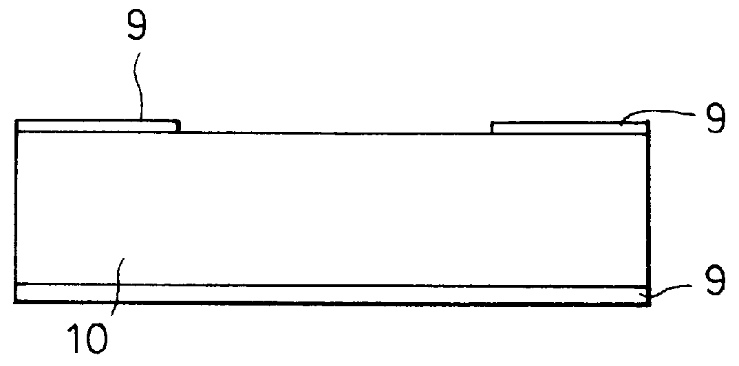
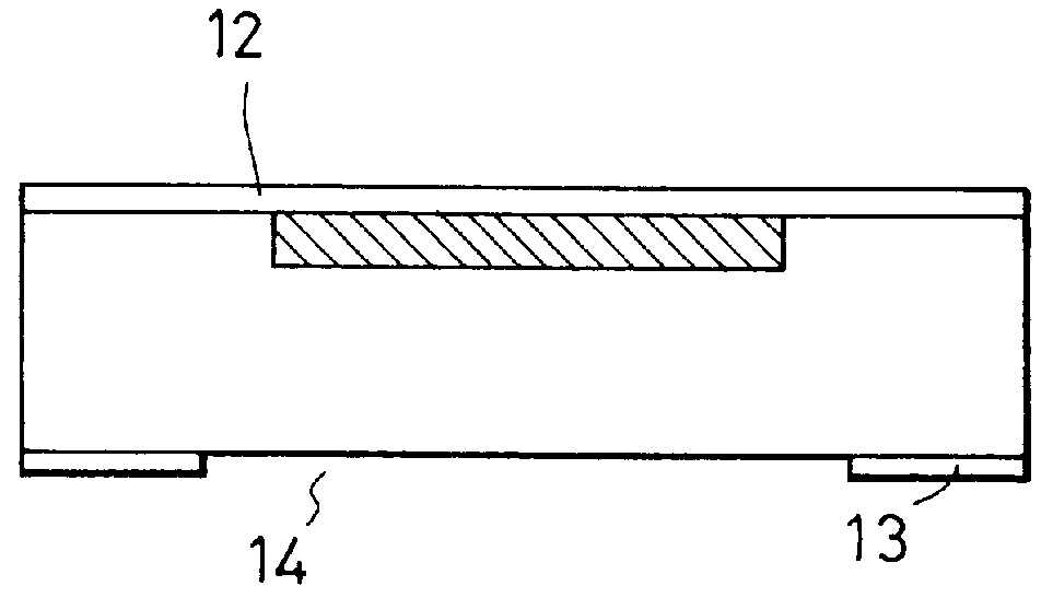
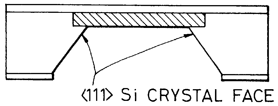
FIG. 1 is a cross-section view illustrating the processing steps of producing a through-hole according to the present invention. FIG. 2 is a top view and cross-sectional view of a substrate on which there is provided a porous silicon layer serving as an embedded dummy layer 11 by which the through-hole is produced. FIG. 3A is a perspective view illustrating an example of the characteristic structure of a through-hole seen from its cross section. As shown in FIGS. 3A and 3B, the through-hole according to the present invention is characterized in that it has a bent shape in cross section unlike the conventional through-hole shown in FIG. 20 having a trapezoidal shape in cross section. With the method according to the invention, it is possible to control the cross-sectional shape of the through-hole as shown in FIGS. 3A and 3B by properly changing the etching time. This makes it possible to control the fluid conductance of a nozzle surrounded by the (111) crystal surfaces to a desired ...
second embodiment
FIG. 4 is a cross-sectional view illustrating the processing steps of producing a through-hole according to the present invention. FIG. 5 is a top view and cross-sectional view of a substrate on which there is provided a porous silicon layer serving as a dummy layer 11 by which the through-hole is produced. FIG. 6A is a perspective view illustrating an example of the characteristic structure of a through-hole seen from its cross section. As shown in FIGS. 6A to 6C, the through-hole according to the present invention is characterized in that it has a bent shape in cross section unlike the conventional through-hole shown in FIG. 20 having a trapezoidal shape in cross section. In the production method according to the invention, it is possible to form the through-hole into a desired shape in cross section by controlling the etching time such that the cross section has either an outward-bent shape or an inward-bent shape as shown in FIGS. 6A to 6C. This makes it possible to control the ...
third embodiment
FIG. 7 is a top view and cross-sectional view of a substrate on which an embedded dummy layer was formed in accordance with the third embodiment of the present invention. In this embodiment, as shown in FIG. 7, the pattern of the embedded dummy layer seen from the upper side of the substrate has the shape of a square each side of which has a length of d2. A though-hole was produced using a similar process to that employed in the first embodiment except that a back-side opening was formed such that it is offset from the (110) orientation by an angle of .alpha.. In this specific embodiment, .alpha. was set to 1.degree.. d2 and .delta. determined by the size of the back-side opening have relationship given by replacing d1 in inequality (3) by d2.
At the principal surface of the substrate, the opening part of the produced through-hole had the shape of a square each side of which had a length d substantially equal to d2. That is, the length d was determined by the shape of the embedded du...
PUM
| Property | Measurement | Unit |
|---|---|---|
| thickness | aaaaa | aaaaa |
| diameter | aaaaa | aaaaa |
| diameter | aaaaa | aaaaa |
Abstract
Description
Claims
Application Information