

Shallow trench isolation method utilizing combination of spacer and fill
a technology of spacer and filling, applied in the direction of basic electric elements, electrical equipment, semiconductor devices, etc., can solve the problem of difficult filling of oxid
- Summary
- Abstract
- Description
- Claims
- Application Information
AI Technical Summary
Benefits of technology
Problems solved by technology
Method used
Image

Examples
Embodiment Construction
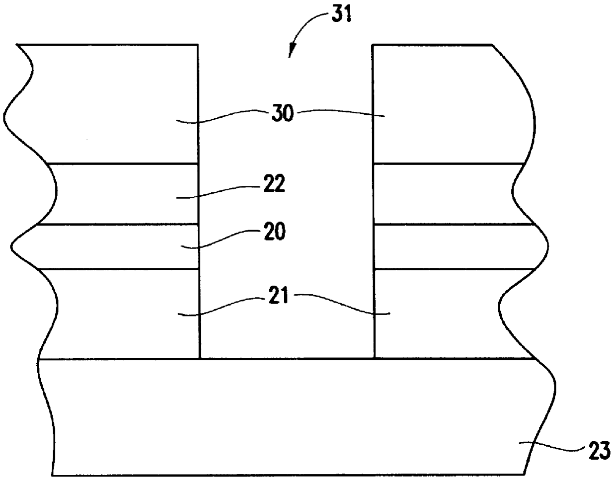
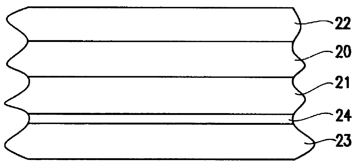
FIG. 1 shows an initial semiconductor structure for forming a shallow trench isolation region in accordance with the present invention. A pad oxide layer 24 and a pad silicon nitride (SiN) layer 21 are formed on a silicon substrate 23 using conventional methods. In regions where deep trench capacitor regions do not exist, a densified tetraethylorthosilicate (TEOS) layer 20 is formed optionally on the pad silicon nitride layer 21. This structure is covered with an insulating boron silicate glass (BSG) hardmask layer 22 before any active area lithography. One skilled in the art would understand that the above mentioned layers are illustrative only and are not meant to limit the scope of the invention. Further, the semiconductor structure may include additional layers not mentioned.
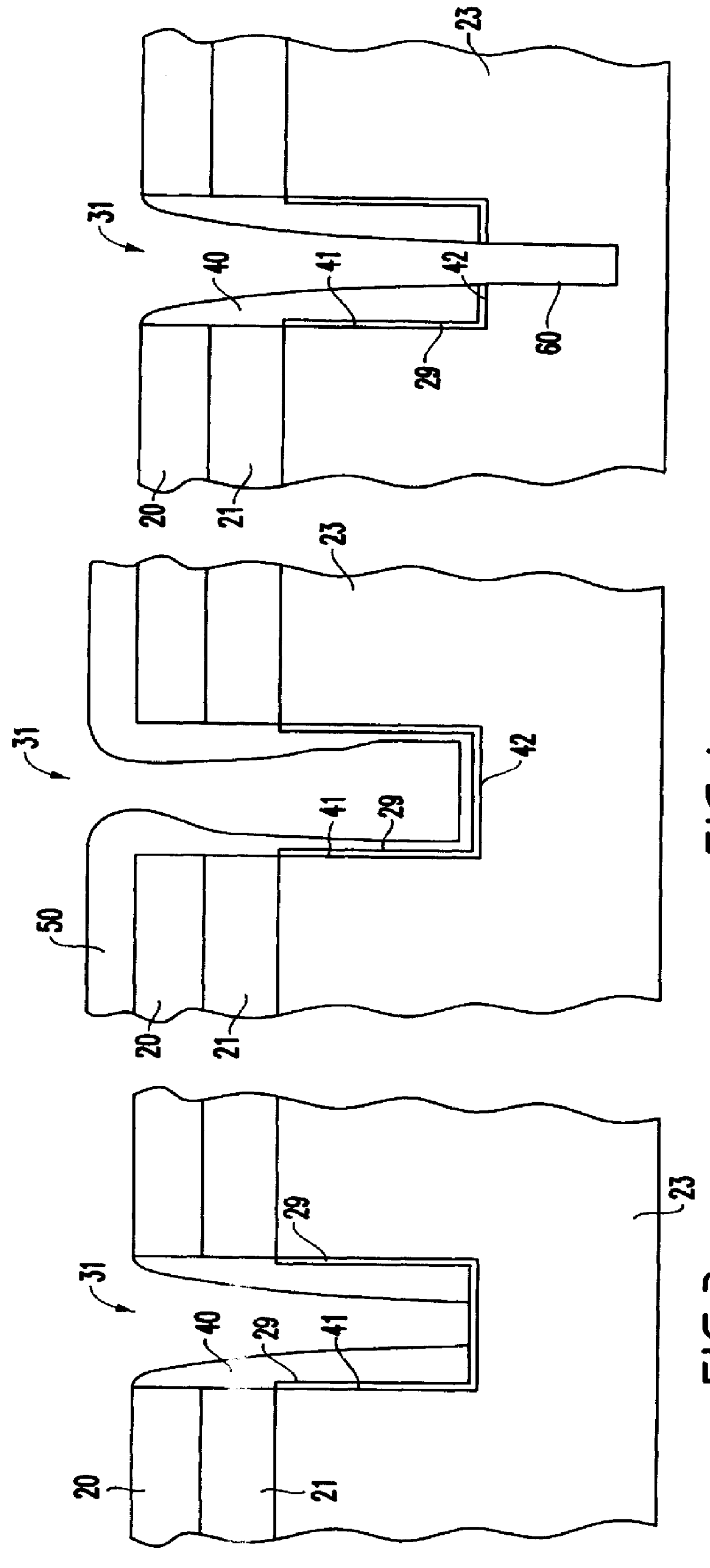
FIG. 2 shows a conventional photoresist 30 placed on the BSG hardmask layer 22. The photoresist 30 defines the active area and the isolation trench region 31 when the BSG hardmask layer 22, the TEOS layer 20...
PUM
 Abstract
Description
Claims
Application Information