Method of making an ultra thin silicon nitride film

a silicon nitride film and ultra-thin technology, applied in the field of semiconductor processing, can solve the problems of reducing device performance, affecting device performance, and affecting device operation,

Inactive Publication Date: 2000-11-21
GLOBALFOUNDRIES INC
View PDF7 Cites 161 Cited by
  • Summary
  • Abstract
  • Description
  • Claims
  • Application Information

AI Technical Summary

Problems solved by technology

As process technologies scaled below about 2.0 .mu.m, a series of design difficulties arose stemming from the semiconductor physics associated with short-channel devices.
Hot carrier effects and subthreshold leakage currents become much more problematic in short channel devices, such as modem field effect transistors in sub-2.0 .mu.m processing.
If not compensated for through processing techniques or other means, such effects can either reduce device performance or lead to device failure or both.
However, the scaling of silicon dioxide gate dielectric layers has introduced another set of problems.
To begin with, very thin silicon dioxide layers have been historically difficult to fabricate with a consistent thickness across a given wafer, from wafer to wafer and from lot to lot.
In addition, as the thickness of silicon dioxide is scaled downward, the potential for reliability problems associated with dielectric breakdown and hot and cold carrier injection degradation increases.
Hot and cold carrier degradation can significantly reduce device performance, while dielectric breakdown can lead to complete device failure.
One potential cause of carrier injection and potential dielectric breakdown is thought to occur as a result of interface traps near the Si--SiO.sub.2 interface.
Independent of the exact physical cause of carrier injection, the empirical result for very thin oxides may be gate leakage currents and / or catastrophic device failure.
Another difficulty associated with very thin conventional gate oxides is polysilicon depletion.
If the amount of boron diffused is sufficiently high, the electrical performance of the field effect transistor may be severely degraded due to polysilicon depletion.
Such films have relatively high tensile stresses (on the order of about 1-2.times.10.sup.10 dynes / cm.sup.2), and the high temperature required for their fabrication consumes thermal budget.
Furthermore, adequate control of film thickness uniformity for thicknesses under about 50 .ANG. has proven to be difficult.
The problem is thought to stem from the high silane flow rates and the sequence of plasma excitation and silane flow used in current processes.
Higher silane flow rates generally speed the silicon nitride forming reaction and make the task of thickness control more difficult.
Exciting the plasma prior to silane flow can cause the resulting silane-ammonia plasma to exhibit instability, which produces variations in film thickness.
The aforementioned process limitations associated with nitride films apply in this context as well.
Furthermore, the conventional gate oxide growth process used to fabricate these types of composite layers is not self-limiting and thus somewhat difficult to control, particularly where very thin oxides are required.

Method used


Image

  • Method of making an ultra thin silicon nitride film
  • Method of making an ultra thin silicon nitride film
  • Method of making an ultra thin silicon nitride film

Examples


Embodiment Construction

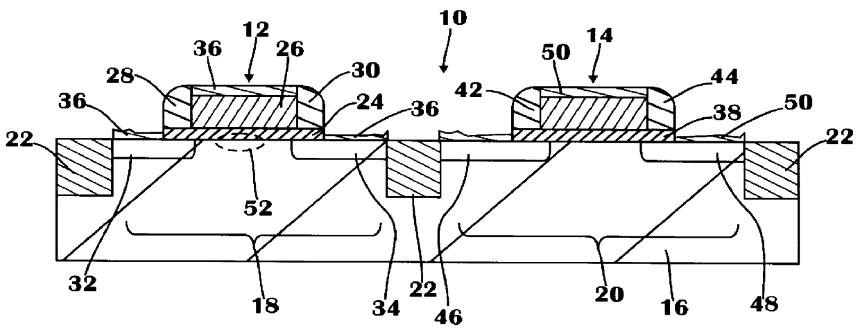
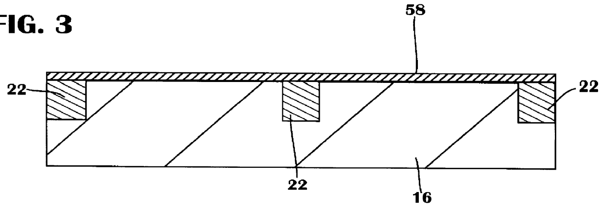
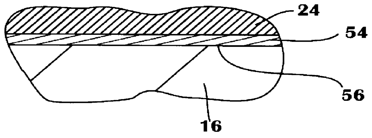
In the drawings described below, reference numerals are generally repeated where identical elements appear in more than one figure. FIG. 1 depicts a cross-sectional view of an integrated circuit 10 that includes a plurality of transistors and other devices. Two of the transistors are depicted and designated 12 and 14 respectively. The transistors 12 and 14 are implemented on a semiconductor substrate 16. Only a very small portion of the substrate 16 is visible in FIG. 1. The transistor 12 is implemented on an active area 18 of the substrate 16 and the transistor 14 is implemented on an adjacent active area 20 of the substrate 16. The active areas 18 and 20 are electrically isolated laterally by isolation structure 22. The transistor 12 is provided with a gate insulating layer 24 positioned on the substrate 16 and a gate electrode 26 positioned on the gate insulating layer 24. The gate electrode 26 is bracketed by a pair of insulating spacers 28 and 30 which are positioned on portion...


PUM

PropertyMeasurementUnit
dielectric constantaaaaaaaaaa
thicknessesaaaaaaaaaa
thicknessaaaaaaaaaa

Abstract

Various methods of fabricating a circuit structure utilizing silicon nitride are provided. In one aspect, a method of fabricating a circuit structure is provided that includes forming a silicon nitride film on a silicon surface, annealing the silicon nitride film in an ammonia ambient and annealing the silicon nitride film in a nitrous oxide ambient to form a thin oxide layer at an interface between the silicon nitride film and the silicon surface. The process of the present invention enables the manufacture of thin silicon nitride films with highly uniform morphology for use as gate dielectrics or other purposes. The thin oxide film is self-limiting in thickness and improves differential mechanical stresses.

Description

1. Field of the InventionThis invention relates generally to semiconductor processing, and more particularly, to a method of fabricating a silicon nitride film on a substrate.2. Description of the Related ArtScaling of field effect transistor devices has historically been, and continues to be a fundamental goal in the semiconductor fabrication industry. The continual drive toward higher circuit density has been fueled by demands from ordinary consumers, industry, government and the military for ever increasing speed, capability and miniaturization of electronic products, as well as the desire of semiconductor manufacturers to reduce manufacturing costs. Scaling efforts have thus far been highly successful. Three micron processing, considered state of the art a little more than a decade ago, has given way to sub-micron processing.As in many aspects of semiconductor processing, current scaling efforts involve a set of trade-offs between higher packing density and better performance, a...

Claims


Application Information

Patent Timeline
Patent Type & Authority Patents(United States)
IPC IPC(8): H01L21/28H01L21/02H01L21/318H01L29/51
CPCH01L21/28185H01L21/28202H01L29/518Y10S438/958H01L21/3185H01L21/02274H01L21/0214H01L21/02211H01L21/0217H01L21/02362H01L21/02337
Inventor SUN, SEY-PINGGARDNER, MARK I.SONG, SHENGNIAN
Owner GLOBALFOUNDRIES INC
Why Eureka
Try Eureka