Programmable interconnect architecture

a programming interface and interconnection technology, applied in the direction of logic circuits using specific components, pulse techniques, instruments, etc., can solve the problems of large current required for operation of usable links, inflexible use of an integrated circuit and/or plane combination of gates to implement logic functions, and not well suited to random logic functions. , to achieve the effect of high complexity and performan

Inactive Publication Date: 2000-12-12
ACTEL CORP
View PDF329 Cites 56 Cited by
  • Summary
  • Abstract
  • Description
  • Claims
  • Application Information

AI Technical Summary

Benefits of technology

An object of the invention is to provide a user programmable circuit with a flexible interconnect architecture that allows the implementation of field programmable semi-custom integrated circuits with high complexity and performance.
Connections to the wiring channels are made by a normally-open programmable element situated at the intersection of any two wires to be connected. To make a connection, the programmable element is programmed, resulting in a low impedance electric connection between the two wires. To provide more efficient utilization of the wiring channels, a plurality of these programmable elements are used to segment the vertical and horizontal channels into shorter wire lengths. These segments may be joined together to form longer wire connections by programming the programmable elements or left as is to provide independent segment wire lengths and allow the same wiring channel position-to be used Several times for different circuit connections. According to the present invention, different segment lengths are employed for efficient connectability.

Problems solved by technology

Gate arrays are therefore mask programmable and not user programmable.
Such fusible links often require large current to operate and require extra area on the integrated circuit.
First, the use of an AND plane / OR plane combination of gates to implement logic functions is inflexible and is not well suited to the requirement of random logic functions.
Second, the utilization factor of such an array is quite low and a large number of gates are wasted.
Third, the integrated circuit chip area-per-functional capability is usually quite high.
However, their main disadvantage is that they are mask programmable and not user programmable.
This results in much higher costs to develop the circuit and its unique mask patterns, and a long turn-around time to order and receive integrated circuit chips.

Method used


Image

  • Programmable interconnect architecture
  • Programmable interconnect architecture
  • Programmable interconnect architecture

Examples


Embodiment Construction

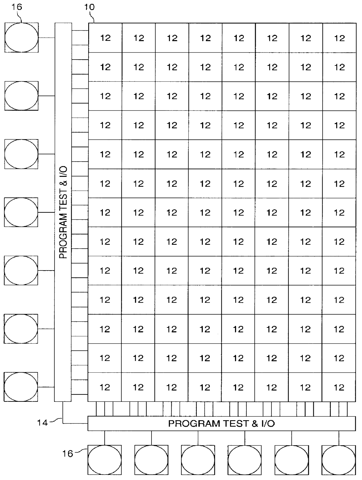
Referring first to FIG. 1a, a block diagram of one embodiment of the user programmable array circuit, one may see that the circuit contains an array block 10 organized into columns and rows of individual circuit modules 12; the program, test, and input / output (I / O) blocks 14 and the I / O pads 16. The number of columns or rows of modules 12 may be chosen to accommodate the desired array size. The program, test, and I / O blocks 14 are used to program all the required vertical and horizontal connections in the array, test the array logic and wiring channels, provide connections between the I / O pads and the array circuitry, and provide a mechanism to select any internal node as a test point to be observed from the I / O pads 16.

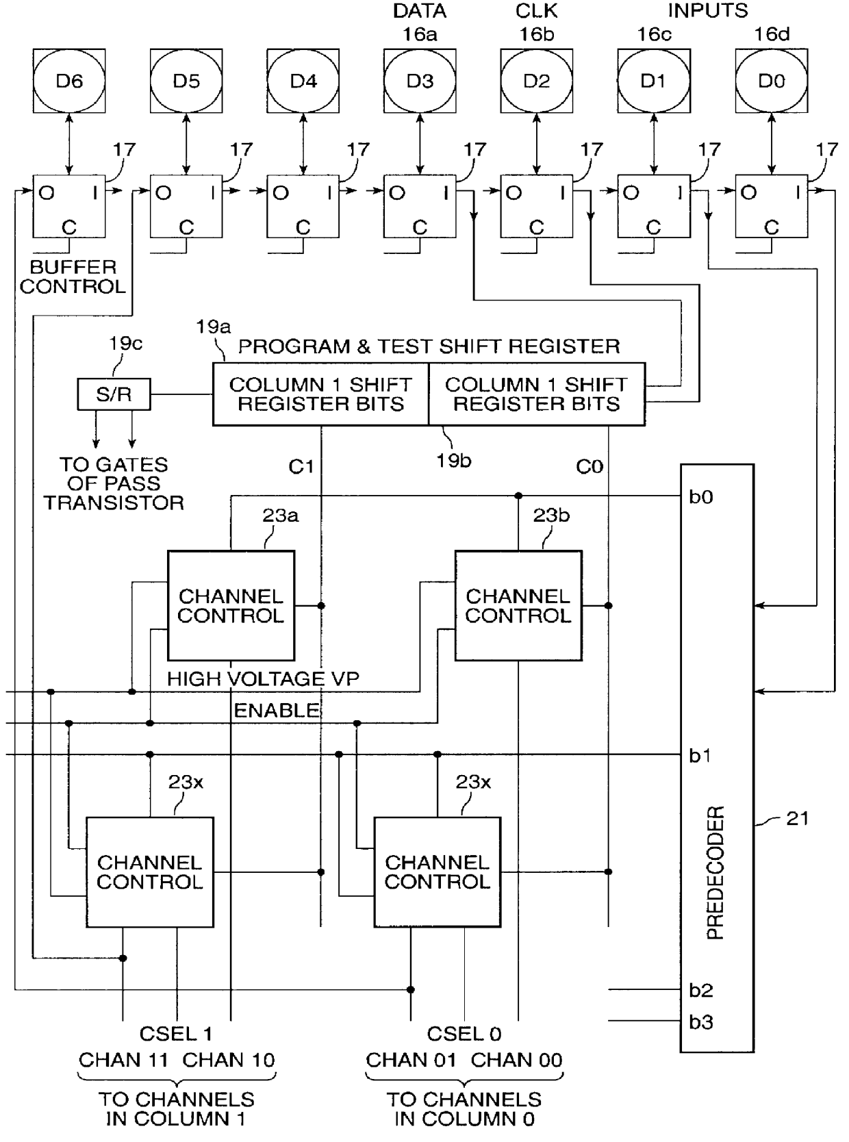
A preferred embodiment of the program, test and I / O logic 14 is shown in FIG. 1b. The figure illustrates how the circuit is used to program a plurality of channels using the example of channels situated in two different columns to explain circuit functionality. From ...


PUM


Abstract

A user-programmable interconnect architecture, which may be used for logic arrays for digital and analog system design, is disclosed. In one embodiment, a plurality of logic cells or modules in a matrix are connected by vertical and horizontal wiring channels. The wiring channels may in turn be programmed by the user to interconnect the various logic cells to implement the required logic function. The wiring channels comprise wiring segments connected by normally open programmable. Elements situated at the intersection of any two segments to be connected.

Description

1. Field of the InventionThe present invention relates to integrated circuit technology. More specifically, the present invention pertains to user-configurable interconnections for array logic and other circuitry.2. The Prior ArtAn integrated circuit uses a network of metal interconnects between the individual semiconductor components which are patterned with standard photolithographic processes during wafer fabrication. Multiple levels of metalized patterns may be used to increase the flexibility of the interconnects. For example in very Large Scale Integration higher density and more complex wiring network are needed.It has long been recognized that a user programmable interconnect technique or manufacturer programmability just prior to shipment would allow lower tooling costs and faster delivery time. On technique to accomplish this uses lasers to make or break pre-patterned metal interconnects between an array of logic cells. This is usually performed on the finished wafer prior...

Claims


Application Information

Patent Timeline
Patent Type & Authority Patents(United States)
IPC IPC(8): H01L25/00H03K19/177G01R31/28G01R31/3185
CPCG01R31/2884G01R31/318516H03K19/17736H03K19/17704G01R31/318519
Inventor GAMAL, ABBAS ELEL-AVAT, KHALED A.MOHSEN, AMR
Owner ACTEL CORP
Why Eureka
Try Eureka