Site-selective electrochemical deposition of copper

a technology of electrochemical deposition and site selection, applied in the field of site selection electrochemical deposition of copper, electrochemical deposition, etc., can solve the problems of high susceptibility to stress migration, poor electromigration characteristics of aluminum, and high cost of aluminum,

Inactive Publication Date: 2001-01-02
ADVANCED MICRO DEVICES INC
View PDF8 Cites 62 Cited by
  • Summary
  • Abstract
  • Description
  • Claims
  • Application Information

AI Technical Summary

Problems solved by technology

However, because aluminum has poor electromigration characteristics and high susceptibility to stress migration, it is typically necessary to alloy aluminum with other metals.
The one criterion that is most seriously compromised by the use of aluminum for interconnects is that of conductivity.
Silver, for example, is relatively expensive and corrodes easily, and gold is very costly and difficult to etch.
ly. However, copper is exceedingly difficult to etch in a semiconductor environm
This increases the cost of the raw materials and the amount of processing needed to remove the copper from undesired areas when compared to a method that enables a copper layer to be selectively deposited only to desired areas.
However, the conductive properties of barrier layer 320 are limiting when the barrier layer 320 is used as a conductive coupling between contact openings 310, and this is problematic.
However, because there is the formation of a dielectric material mask 325 after contact openings 310 have been etched, the dielectric material mask 325 is difficult to remove from contact openings 310, particularly from deep openings, and this is problematic.
Such photoresist and / or masking materials are difficult to remove from openings, particularly from deep openings.

Method used


Image

  • Site-selective electrochemical deposition of copper
  • Site-selective electrochemical deposition of copper
  • Site-selective electrochemical deposition of copper

Examples


first embodiment

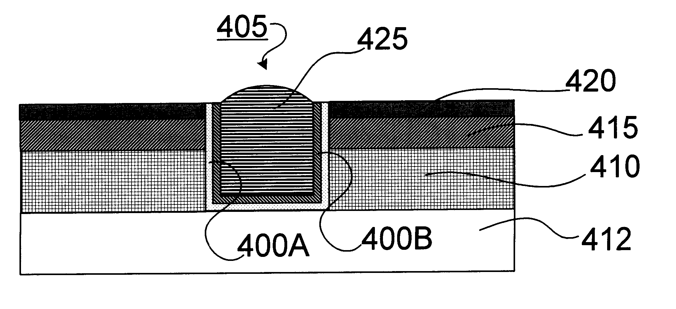
As shown in FIG. 4C, copper 425 may then be selectively electrochemically deposited only in the opening 405 and not on the insulating layer 420. Alternatively, any other suitable material besides copper may equivalently and interchangeably be selectively electrochemically deposited only in an opening in a similar manner. This first embodiment of a method for selectively electrochemically depositing copper according to the present invention, as illustrated in FIGS. 4A-4C, may be appropriate to both single-damascene copper process flows and dual-damascene copper process flows.

second embodiment

a method for selectively electrochemically depositing copper according to the present invention is illustrated in FIGS. 5A-5H. As shown in FIG. 5A, a conductive layer 500 may be formed (for example, by being deposited) on a layer of dielectric material 505. The layer of dielectric material 505 is formed (for example, by being deposited) on another dielectric layer 507. The layer of dielectric material 505 may be an interlayer dielectric (ILD). The other dielectric layer 507 has an intermetal via connection 509 disposed therein. The conductive layer 500 is capable of having an insulating layer 510 (shown in phantom in FIG. 5A) formed on an upper surface of the conductive layer 500. The conductive layer 500 may be conductive or may be capable of being made conductive. The other dielectric layer 507 is disposed on a structure layer 511. The structure layer 511 may be an underlayer of semiconducting material, such as a silicon substrate or wafer, for example, or, alternatively, may be a...

third embodiment

a method for selectively electrochemically depositing copper according to the present invention is illustrated in FIGS. 6A-6J. As shown in FIG. 6A, a first masking layer 600 may be formed (for example, by being deposited and patterned) on a first layer of dielectric material 605. The first layer of dielectric material 605 may be disposed on a structure layer 607. The structure layer 607 may be an underlayer of semiconducting material, such as a silicon substrate or wafer, for example, or, alternatively, may be an underlayer of semiconductor devices, such as a layer of metal oxide semiconductor field effect transistors (MOSFETs), and the like, and / or a metal interconnection layer or layers and / or an interlayer dielectric layer or layers, and the like. As shown in FIG. 6B, a second layer of dielectric material 610 may be formed (for example, by being deposited) on the first layer of dielectric material 605.

As shown in FIG. 6C, a conductive layer 615 may be formed (for example, by bein...


PUM

PropertyMeasurementUnit
melting pointaaaaaaaaaa
thicknessaaaaaaaaaa
constant temperatureaaaaaaaaaa

Abstract

A method is provided for selectively electrochemically depositing copper. The method includes forming a layer of dielectric material above a structure layer, forming a conductive layer above the layer of dielectric material and forming an opening in the conductive layer and the layer of dielectric material. The method also includes selectively forming at least one barrier metal layer and a copper seed layer only in the opening, the at least one barrier metal layer and the copper seed layer being conductively coupled to the conductive layer. The method further includes forming an insulating layer above the conductive layer, and selectively electrochemically depositing copper only in the opening.

Description

1. Field of the InventionThis invention relates generally to semiconductor fabrication technology and, more particularly, to electrochemical deposition processes for filling contact openings and vias and creating interconnect lines with metal.2. Description of the Related ArtThe ideal interconnect conductor for semiconductor circuitry will be inexpensive, easily patterned, have low resistivity, and high resistance to corrosion, electromigration, and stress migration. Aluminum is most often used for interconnects in contemporary semiconductor fabrication processes primarily because it is inexpensive and easier to etch than, for example, copper. However, because aluminum has poor electromigration characteristics and high susceptibility to stress migration, it is typically necessary to alloy aluminum with other metals.As semiconductor device geometries shrink and clock speeds increase, it becomes increasingly desirable to reduce the resistance of the circuit metallization. The one crit...

Claims


Application Information

Patent Timeline
Patent Type & Authority Patents(United States)
IPC IPC(8): C25D5/02C25D5/10H01L21/70H01L21/768
CPCC25D5/022C25D5/10H01L21/76879
Inventor BROWN, THOMAS M.HYMES, STEPHEN W.
Owner ADVANCED MICRO DEVICES INC
Why Eureka
Try Eureka