Method and apparatus for forming optical gratings

a technology of optical gratings and gratings, applied in the field of methods and apparatus for forming optical gratings, can solve the problems of difficult masking, difficult to balance the diffraction efficiency of the different gratings, and difficulty in fabricating highly efficient (>90%) diffractive structures

Inactive Publication Date: 2001-01-09
ROSSELLA
View PDF22 Cites 48 Cited by
  • Summary
  • Abstract
  • Description
  • Claims
  • Application Information

AI Technical Summary

Problems solved by technology

Fabrication of highly efficient (>90%) diffractive structures is difficult, time consuming and expensive.
Holographic fabrication can yield high diffraction efficiencies, but when the gratings of different pitches are required on the same substrate several problems arise.
1) It is difficult to mask off small areas from exposure; 2) It is difficult to balance the diffraction efficiencies of the different gratings to the specified or desired values; and 3) The process is time consuming, and thus expensive in a manufacturing setting.
A drawback with this approach is that a great deal of light is scattered by these grating devices when no electrical field is applied.
Further, the operating voltages of this device are still very high (>100 volts) and thus silicon driving circuitry is not easy to integrate.
One drawback with this approach is that such embossed

Method used


Image

  • Method and apparatus for forming optical gratings
  • Method and apparatus for forming optical gratings
  • Method and apparatus for forming optical gratings

Examples


Embodiment Construction

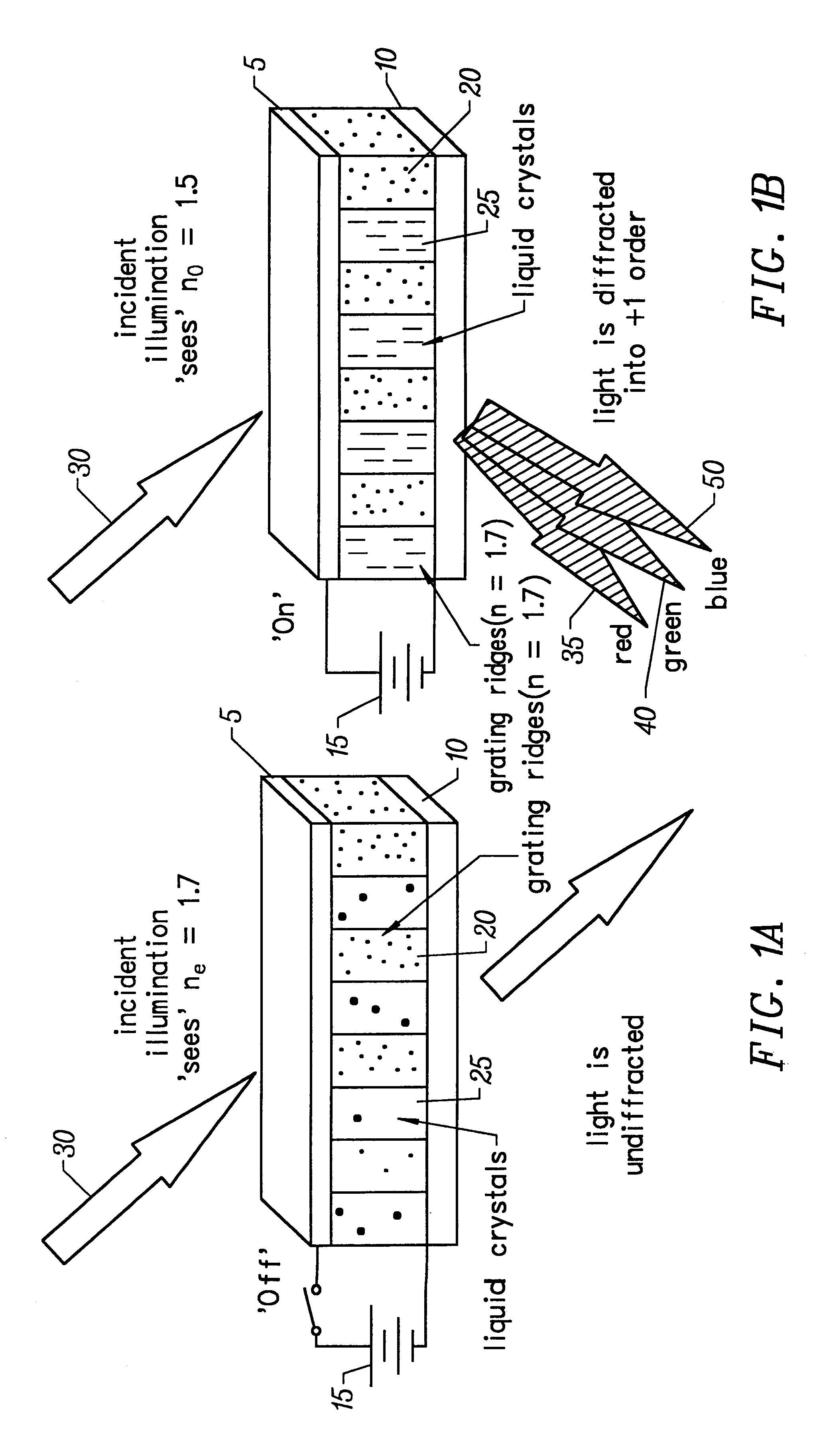
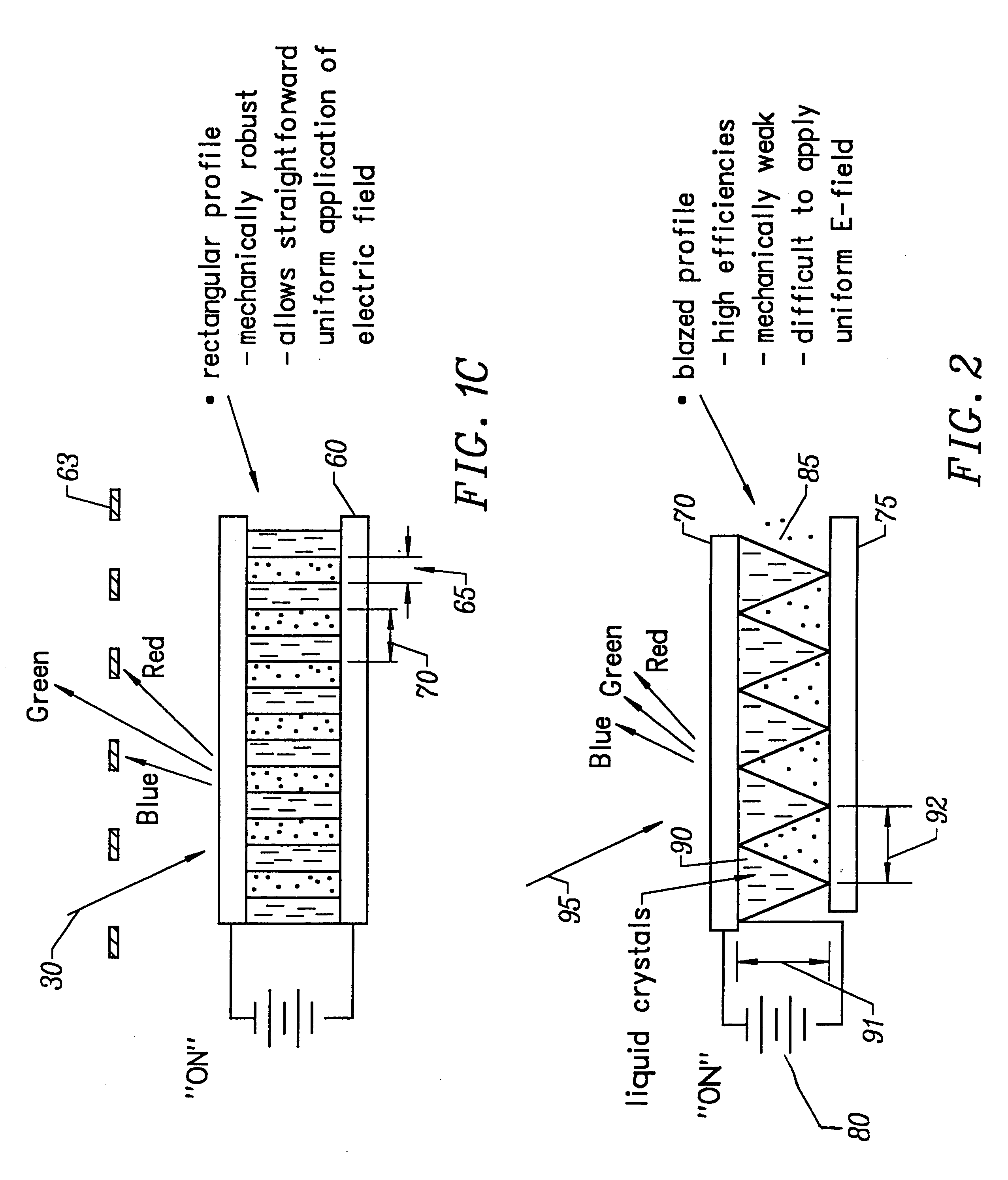
I. Virtual Blaze Gratings

A. Sidewall Configurations

1. Off-Center Configurations

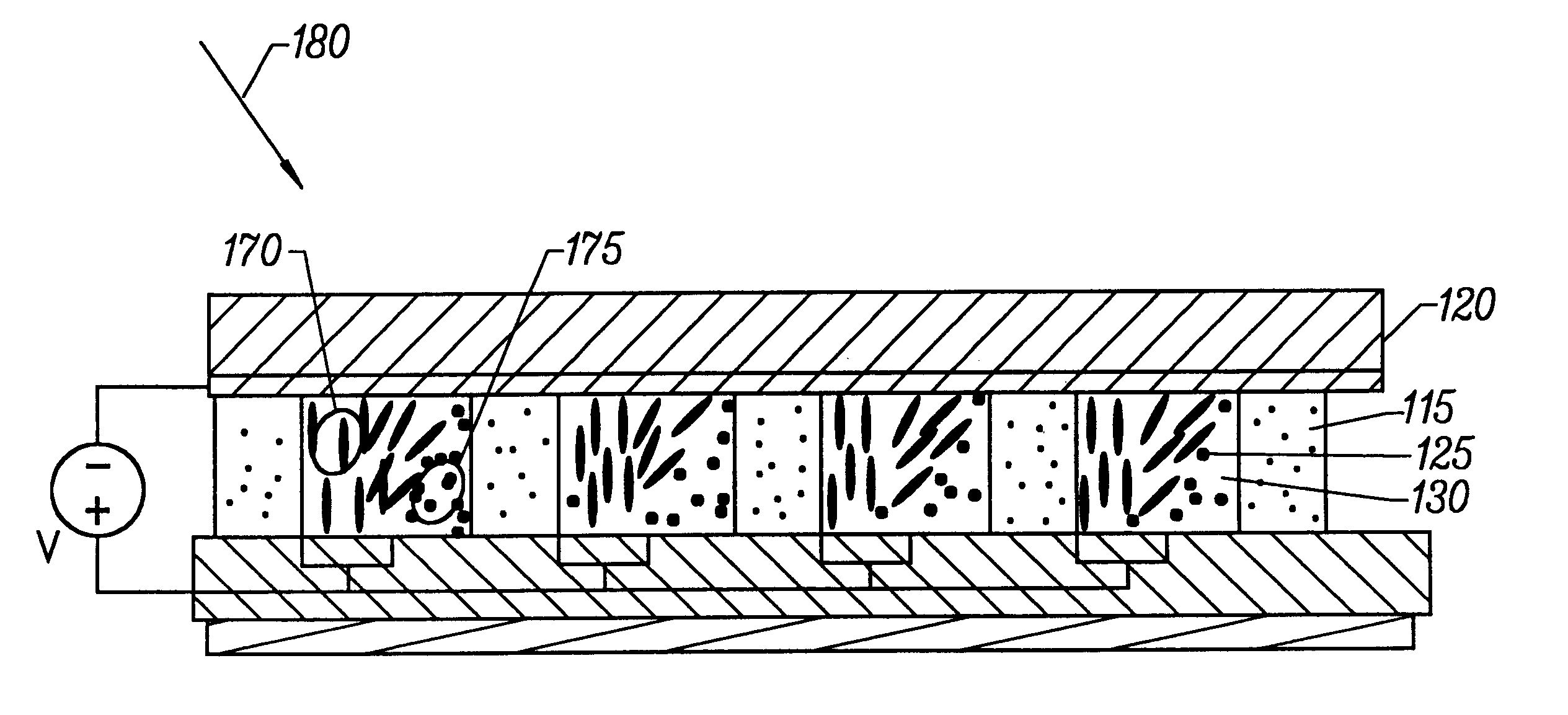
FIG. 3a illustrates a cross-section of a structure used in an embodiment of the present invention. FIG. 3a includes a structure 98 including substrate 100, an insulating layer 105, electrodes 110, insulating walls 115, a conductive layer 120, and cavities 125, defining cell regions, bounded by at least the above materials. Cavities 125 include material 130, and conductive layer 120 includes a conductive material 145 disposed on transparent substrate 150.

Substrate 100 is typically used when operating the invention in a reflective mode, i.e. where incident light does not pass through structure 98. In a transmissive mode, i.e. where incident light passes through structure 98, substrate 100 may be eliminated. Substrate 100 typically comprises a semiconductor substrate such as silicon, although other semiconductor substrates and other substrate materials are within alternative embodiments of the present invent...


PUM


Abstract

An apparatus for redirecting physical energy includes a substrate defining a first boundary of a region, a first electrode defining a second boundary of the region, the second boundary disposed opposite to the first boundary, a second electrode adjacent to the first boundary for cooperating with the first electrode to apply a non-uniform electric field to the region, the non-uniform electric field having electrical field intensities simultaneously including a first electric field intensity and a second electric field intensity, and a layer of material disposed in the region, the layer having a variable index of refraction responsive to the electric field intensities of the non-uniform electric field, the variable index of refraction including a first index of refraction in response to the first electric field intensity and a second index of refraction in response to the second electric field intensity.

Description

The present invention relates to methods and apparatus for redirecting physical energy, in particular, improved methods and apparatus for forming optical gratings for color displays.More specifically, the present invention relates to a light diffracting device with several gratings, each with a different pitch, that is suitable for optical display, light coupling, optical recording, light communications, spectral analysis, among others. More particularly, the device can be simply fabricated on standard micro-electronic foundry lines and allows integration between the diffractive structure and circuitry embedded in the semiconductor wafer, while still achieving high diffraction efficiencies (>90%). The diffraction efficiency of the device can also be optionally modulated by an applied field provided by semiconductor circuitry embedded in the substrate.I. Rectangular GratingsFIGS. 1a and 1b illustrate a typical transmissive mode grating. FIGS. 1a and 1b include transparent electrod...

Claims


Application Information

Patent Timeline
IPC IPC(8): G02F1/03G02F1/13G02F1/1333G02F1/01G02B5/18G02F1/29
CPCG02B5/1828G02B5/1847G02F1/292G02F1/133377G02F1/133707
Inventor JEPSEN, MARY LOUALVELDA, PHILLIP
Owner ROSSELLA
Why Eureka
Try Eureka